Vertical junction pv cells

Inactive Publication Date: 2012-06-21
OFEK ESHKOLOT RES & DEV +1
View PDF8 Cites 28 Cited by
  • Summary
  • Abstract
  • Description
  • Claims
  • Application Information

AI Technical Summary

Benefits of technology

[0077]In an exemplary embodiment of the invention, the cell junctions are thick enough to absorb, for example, at least 70%, 80%, 90% of impinging radiation at wavelengths that significantly interact with the materials used in the junctions. Optionally, the distance of travel required by generated carriers is reduced as compared to stacked cells, for example, being 50%, 30%, 20% or less, o

Problems solved by technology

However, this technology is not very efficient (less than 20% conversion efficiency for commercially available solar panels), and quite expensive (solar electricity today is about four times more expensive than electricity from fossil fuels).
But this growth is fueled by government subsidies and not by a real competitive position in the energy market.
Most notable are:Thin-film cells, which use significantly smaller amounts of the expensive semiconductor material; but they usually offer lower efficien

Method used


Image

  • Vertical junction pv cells
  • Vertical junction pv cells
  • Vertical junction pv cells

Examples


Embodiment Construction

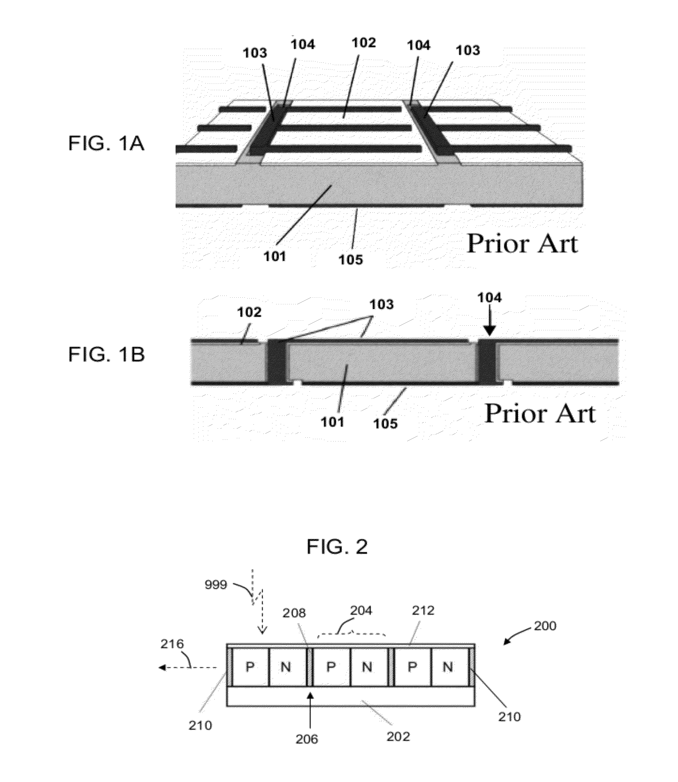
[0191]The present invention, in some embodiments thereof, relates to a photovoltaic cell design and, more particularly, but not exclusively, to a monolithic photovoltaic cell design.

[0192]As used herein, the term ‘monolithic’ implies, without limiting, that functional units such as semiconductor junction are formed in a single piece of material, optionally disregarding auxiliary components attached to the piece.

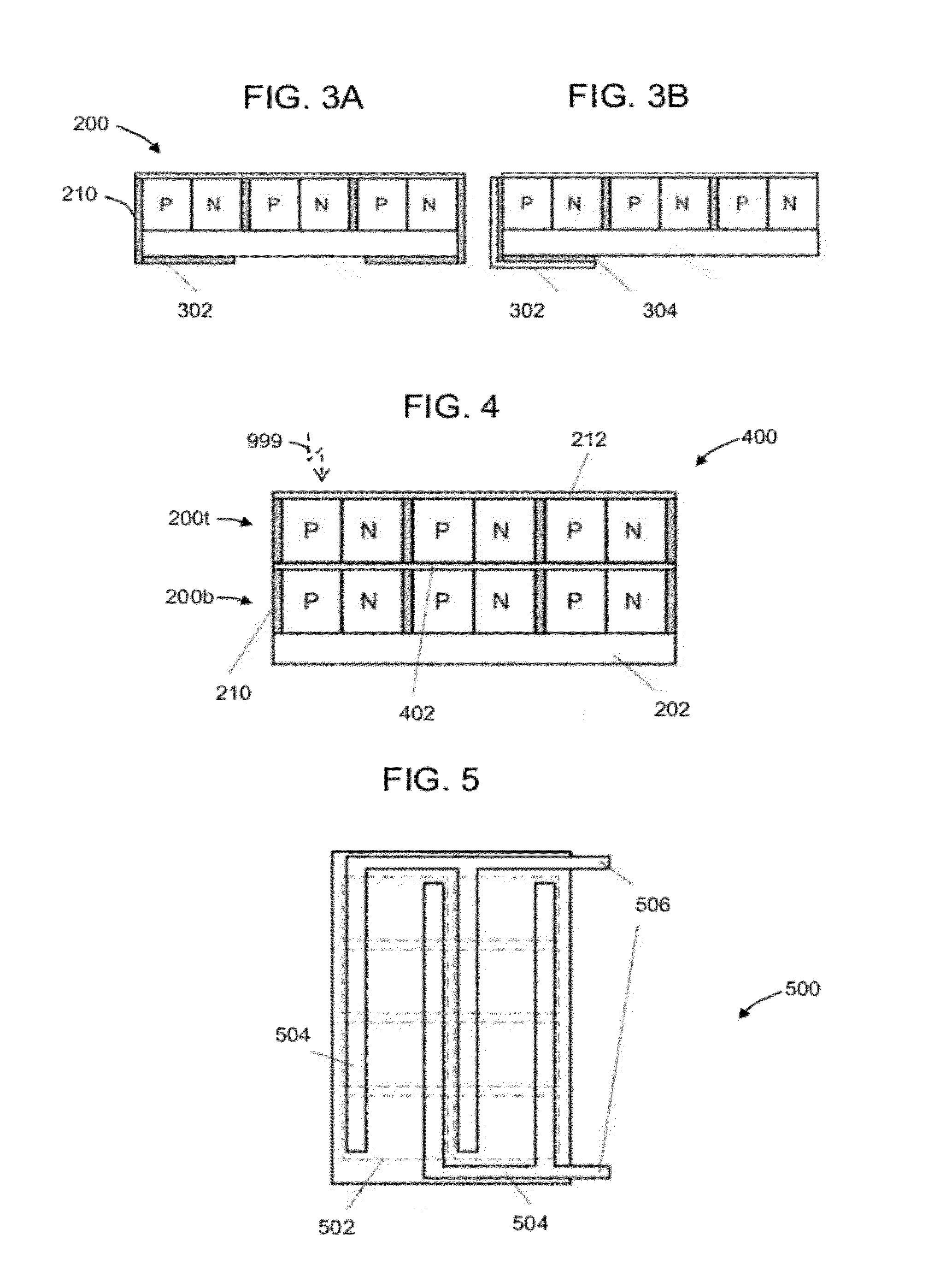
[0193]As used herein, the term ‘semi-monolithic’ implies, without limiting, attaching (e.g. bonding) two or more monolithic units to form a once-piece apparatus or part thereof, optionally disregarding auxiliary components attached to the units or apparatus.

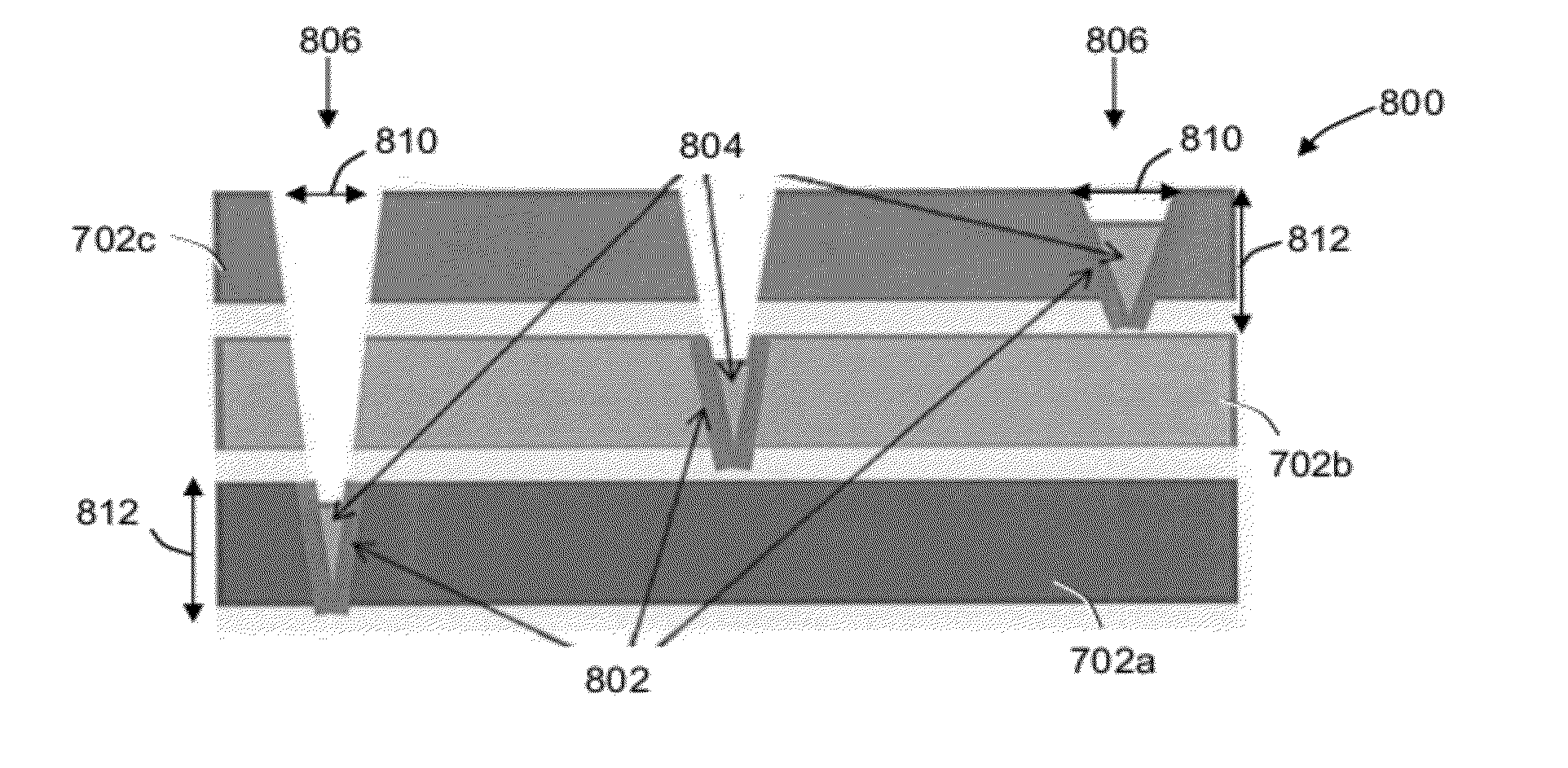
[0194]As used herein, and unless otherwise specified, an intended (designed) radiation incidence angle (also referred to as ‘incident radiation’) is perpendicular to a cell's general surface intended for exposure to the radiation, without precluding or limiting inclined radiation when a cell is exposed to electromagnetic (...


PUM


Abstract

A monolithic semiconductor solar cell including a semiconductor layer including a plurality of pores, wherein walls of the pores are doped, forming vertical junctions between the walls of the pores and a bulk of the semiconductor, the pores each contain a conductor which is in electrical contact with the walls of the pores, and the conductors of the pores are electrically interconnected to provide an output voltage of the solar cell. A monolithic semiconductor solar cell including a semiconductor layer including a plurality of trenches, wherein walls of the trenches are doped, forming vertical junctions between the walls of the trenches and a bulk of the semiconductor, the trenches each contain a conductor which is in electrical contact with the walls of the trenches, and the conductors of the trenches are electrically interconnected to provide an output voltage of the solar cell. Related apparatus and methods are also described.

Description

RELATED APPLICATIONS[0001]This application is a continuation-in-part (CIP) of PCT Patent Application No. PCT / IB2010 / 052196 having International filing date of May 18, 2010, which claims the benefit of priority of U.S. Provisional Patent Application Nos. 61 / 282,184 filed on Dec. 28, 2009, 61 / 272,643 filed on Oct. 15, 2009, and 61 / 179,420 filed on May 19, 2009. The contents of the above applications are all incorporated herein by reference.FIELD AND BACKGROUND OF THE INVENTION[0002]The present invention, in some embodiments thereof, relates to a photovoltaic cell design and, more particularly, but not exclusively, to a monolithic photovoltaic cell design.[0003]The leading solar energy technology is a direct conversion of sunlight to electricity using photovoltaic cells, usually with cells based on single-crystal silicon. However, this technology is not very efficient (less than 20% conversion efficiency for commercially available solar panels), and quite expensive (solar electricity t...

Claims


Application Information

Patent Timeline
IPC IPC(8): H01L31/05H01L31/18
CPCH01L31/0687H01L31/047H01L31/0475Y02E10/544Y02P70/50
Inventor KRIBUS, ABRAHAMROSENWAKS, YOSSISARFATY, RONASEGEV, GIDEON
Owner OFEK ESHKOLOT RES & DEV
Why Eureka
Try Eureka