Active bandgap tuning of graphene for tunable photodetection applications

a graphene and active bandgap technology, applied in the field of photoelectronic devices, can solve the problems of profound limitation of the usefulness of the photodetector devi

Inactive Publication Date: 2012-06-21
STEVENS INSTITUTE OF TECHNOLOGY
View PDF2 Cites 32 Cited by
  • Summary
  • Abstract
  • Description
  • Claims
  • Application Information

AI Technical Summary

Problems solved by technology

This presents a profound limitation of the usefulness of the photodetector device.

Method used


Image

  • Active bandgap tuning of graphene for tunable photodetection applications
  • Active bandgap tuning of graphene for tunable photodetection applications
  • Active bandgap tuning of graphene for tunable photodetection applications

Examples


Embodiment Construction

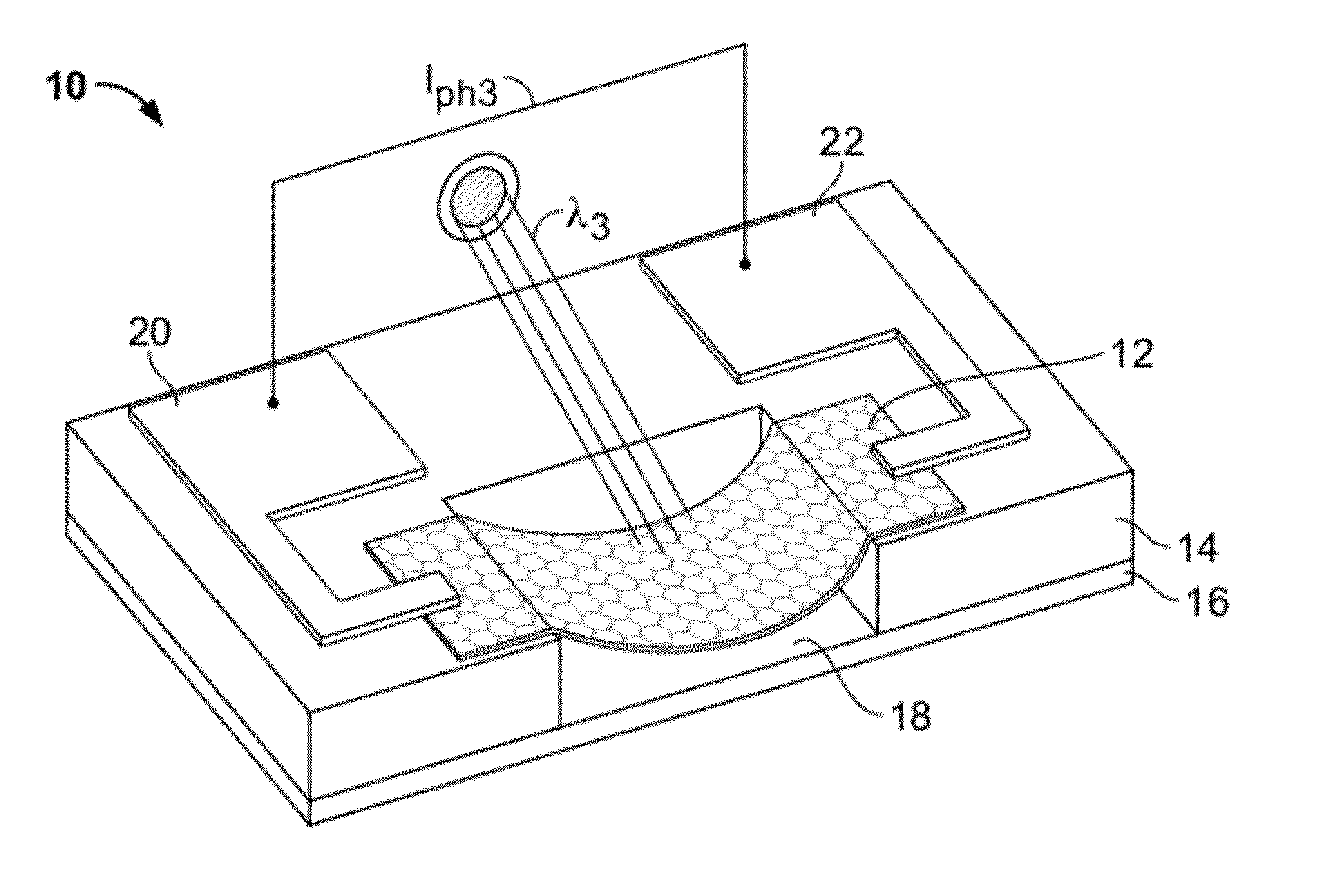
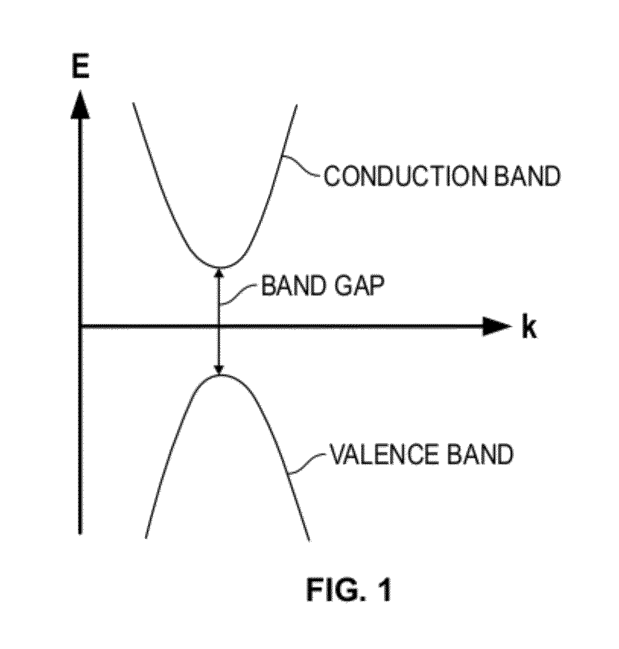
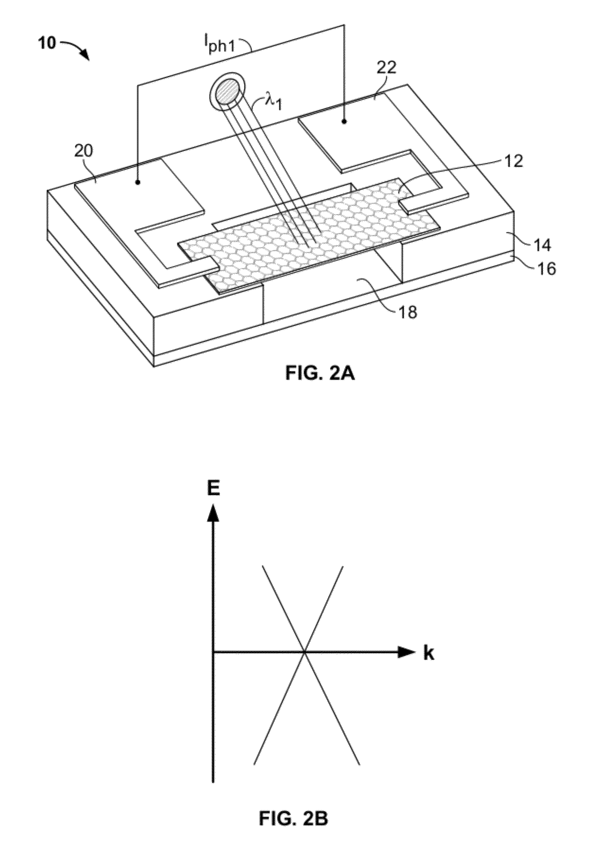
[0020]The present invention provides methods and devices for active in-situ tuning of the bandgap of a photodetector device by inducing strain in the photodetection material. It has particular applicability to materials such as graphene, carbon nanotubes (CNT) or graphene nanoribbons (GNR), but may also be applied to other photodetection materials having electron valence bands that may be altered by inducing strain in the material. The spectral sensitivity of a photodetector that uses such materials can be continuously modulated to detect a wide range of photon energies or wavelengths (A) of the incident light while the device is in operation. The modulation method is hereinafter referred to as “active bandgap tuning” (ABT). Strain induction in graphene, CNT, GNR or other materials can be achieved actively using conventional MEMS actuation techniques, including and not limited to electrostatic actuation, pneumatic actuation or thermal actuation.

[0021]The ABT technique can be advanta...


PUM

PropertyMeasurementUnit
temperaturesaaaaaaaaaa
thicknessaaaaaaaaaa
heightaaaaaaaaaa

Abstract

In a method for adjusting the sensitivity of a photodetector, the bandgap of the photodetection material is adjusted by inducing strain in the photodetection material. Such adjustments can be made in situ and continuously, in a reproducible and repeatable manner. In embodiments of the method, the photodetection material is graphene, carbon nanotubes or graphene nanoribbon. The use of graphene permits a dynamically-adjustable sensitivity over a dynamic range of radiation having wavelengths of 1.38 microns or less, up to at least 60 microns. In an adjustable photodetector, a graphene layer is suspended over a silicon substrate by a layer of an insulating material. Adjusting the voltage across the graphene layer and the silicon substrate induces strain in the graphene layer by electrostatic attraction.

Description

CROSS-REFERENCE TO RELATED APPLICATIONS[0001]This application claims the benefit of U.S. Provisional Patent Application No. 61 / 422,399 filed on Dec. 13, 2011, which is incorporated by reference herein in its entirety.STATEMENT REGARDING FEDERALLY SPONSORED RESEARCH[0002]Not applicable.FIELD OF THE INVENTION[0003]The present invention relates to photoelectronic devices, and more particularly to bandwidth tuning of photodetectors.BACKGROUND OF THE INVENTION[0004]Photodetectors comprise layers of photosensitive materials that can detect incident light of certain photon energies (which may also be expressed as wavelengths) related to the bandgap of the material. A bandgap is defined as the gap, expressed as an energy, between the lowest point of the conduction band and the highest point of the valence band of the material's electron energy dispersion relation (E-k) diagram, an example of which is shown as FIG. 1. Absorption of photons having at least the bandgap energy excites electrons...

Claims


Application Information

Patent Timeline
Patent Type & Authority Applications(United States)
IPC IPC(8): H01L31/028B82Y99/00
CPCY02E10/547B82Y30/00H01L31/09H01L31/028B82Y40/00
Inventor PATIL, VIKRAM ARVINDYANG, EUI-HYEOKSTRAUF, STEFAN
Owner STEVENS INSTITUTE OF TECHNOLOGY
Why Eureka
Try Eureka