Lead pin for package substrate and semiconductor package printed circuit board including the same

Inactive Publication Date: 2012-06-21
SAMSUNG ELECTRO MECHANICS CO LTD
View PDF7 Cites 3 Cited by
  • Summary
  • Abstract
  • Description
  • Claims
  • Application Information

AI Technical Summary

Benefits of technology

[0009]The present invention has been made in an effort to provide a lead pin for a package substrate increasing a bonding area of a head part of the lead pin for a package substrate

Problems solved by technology

As shown in FIG. 1, the head part 100a of the lead pin 100 has a semi-circular shape in the prior art, thereby causing a problem that the bonding strength of the lead pin 100 is degraded.
In particular, in the case of the Pin Grid Array (PGA) type in which the lead pin 100 is mounted on the back surface of the sub

Method used


Image

  • Lead pin for package substrate and semiconductor package printed circuit board including the same
  • Lead pin for package substrate and semiconductor package printed circuit board including the same
  • Lead pin for package substrate and semiconductor package printed circuit board including the same

Examples


Example

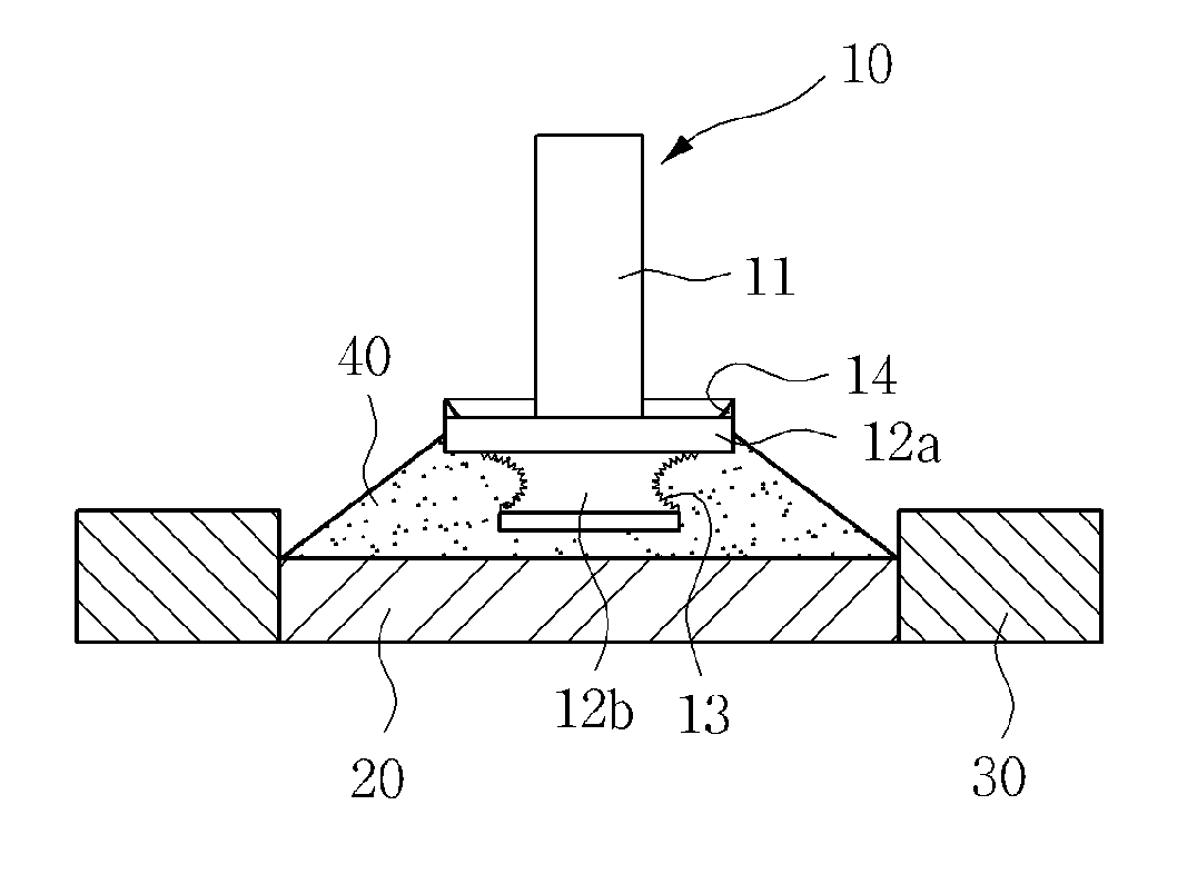
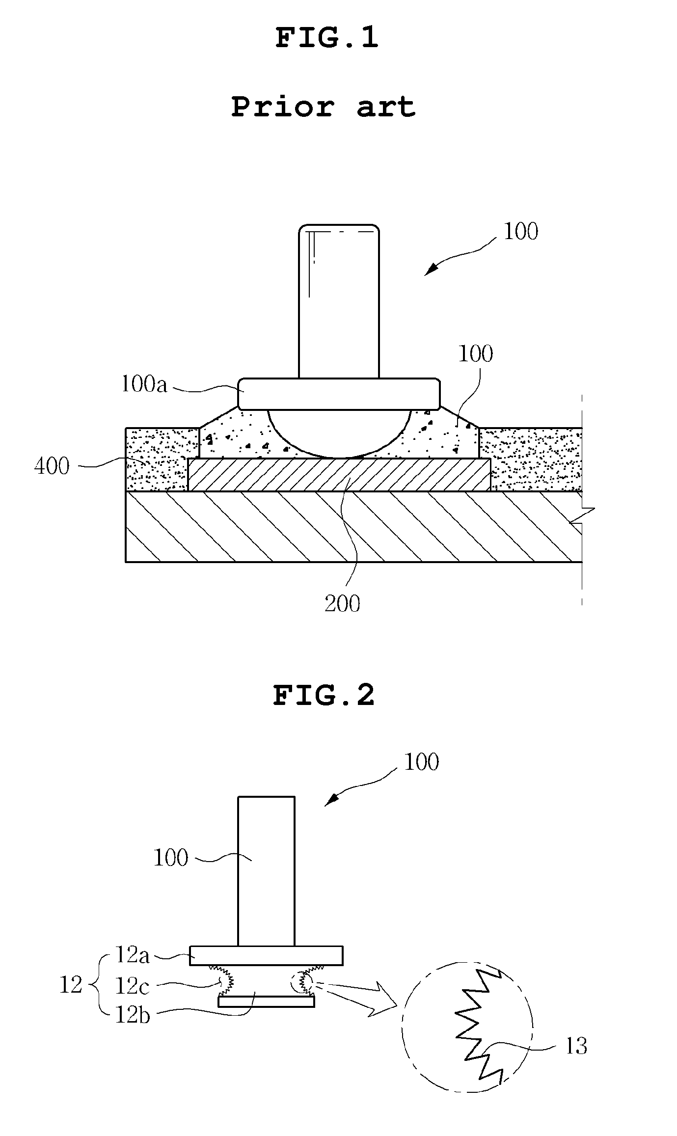
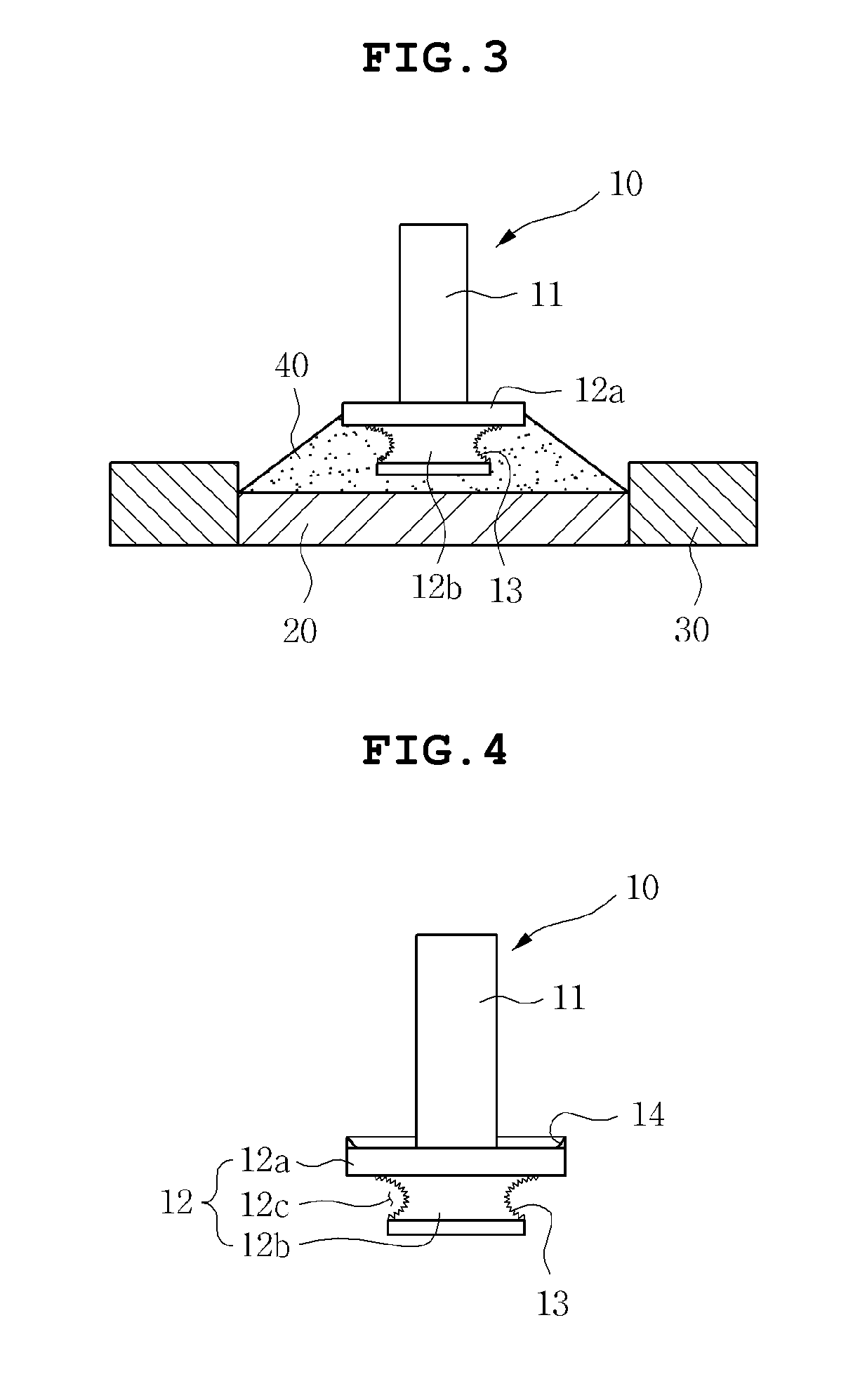
[0025]Various features and advantages of the present invention will be more obvious from the following description with reference to the accompanying drawings.

[0026]The terms and words used in the present specification and claims should not be interpreted as being limited to typical meanings or dictionary definitions, but should be interpreted as having meanings and concepts relevant to the technical scope of the present invention based on the rule according to which an inventor can appropriately define the concept of the tem to describe most appropriately the best method he or she knows for carrying out the invention.

[0027]The above and other objects, features and advantages of the present invention will be more clearly understood from the following detailed description taken in conjunction with the accompanying drawings. In the specification, in adding reference numerals to components throughout the drawings, it is to be noted that like reference numerals designate like components...


PUM


Abstract

Disclosed herein is a lead pin for a package substrate including a connection pin, and a head part including a flange part formed at one end of the connection pin and having one surface bonded to the connection pin and a flat part formed at the other surface of the flange part and having at least one groove formed along an outer circumference thereof. According to the present invention, the grooves are formed along the outer circumference of the flat part of the head part of the lead pin to increase a bonding area, thereby making it possible to increase bonding strength of the lead pin.

Description

CROSS REFERENCE TO RELATED APPLICATION[0001]This application claims the benefit of Korean Patent Application No. 10-2010-0130993, filed on Dec. 20, 2010, entitled “Lead Pin For Package Substrate And Semiconductor Package Printed Circuit Board Including The Same”, which is hereby incorporated by reference in its entirety into this application.BACKGROUND OF THE INVENTION[0002]1. Technical Field[0003]The present invention relates to a lead pin for a package substrate and a semiconductor package printed circuit board including the same.[0004]2. Description of the Related Art[0005]With the development of electronics industry, various types of semiconductor packages have been manufactured. Recently, as the wiring density of a semiconductor package is increased, a semiconductor package substrate in a Pin Grid Array (PGA) type in which a plurality of T-type lead pins are mounted has been widely used as a substrate that connects a package substrate on which an integrated circuit (IC) is moun...

Claims


Application Information

Patent Timeline
IPC IPC(8): H01L23/49H01B5/00
CPCH01L23/49811H01L2924/00013H05K3/4015H05K2201/10318H01L2924/0002H01L2224/13099H01L2224/13599H01L2224/05599H01L2224/05099H01L2224/29099H01L2224/29599H01L2924/00
Inventor LEE, SANG YUL
Owner SAMSUNG ELECTRO MECHANICS CO LTD
Why Eureka
Try Eureka