

Gate driving circuit on array applied to charge sharing pixel
a driving circuit and array technology, applied in the field of driving circuits, can solve the problems of large layout area and complex circuit structure of each shift register, and achieve the effect of simplifying circuit structure and circuit layou
- Summary
- Abstract
- Description
- Claims
- Application Information
AI Technical Summary
Benefits of technology
Problems solved by technology
Method used
Image

Examples
first embodiment
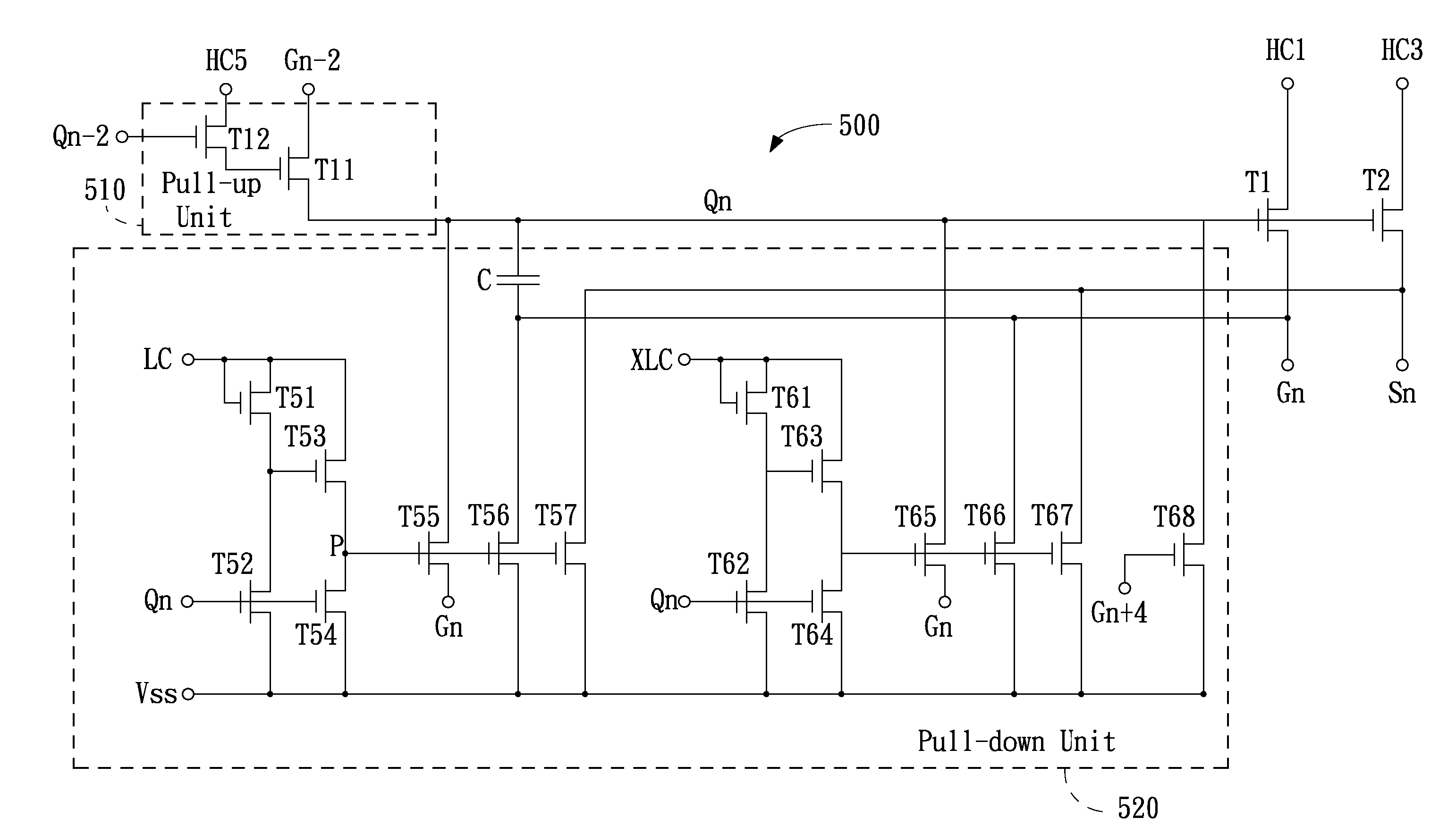
[0056]At the time point t5, the (n+4)th main gate driving signal Qn+4 generates a pulse, the transistor T68 is turned on, the pull-down unit 520 further pulls the nth control signal Qn down to the level of Vss, and the operation of the nth shift register 500 is completed consequently. In the illustrative first embodiment, the predetermined time period is the duration from the time point t2 to the time point t5.
[0057]It is understood that, the signal Sn+4, Gn+5, Sn+5 or Gn+6 instead can be used to pull the nth control signal Qn down to the level of Vss, and the predetermined time period correspondingly is changed.
[0058]It also can be found from the first embodiment, each of the shift registers can generate the mutually non-overlapped main gate driving signal e.g., Gn and sub gate driving signal e.g., Sn.
[0059]As described above, the pull-down unit 520 in the first embodiment can employ other internal circuit structure instead to achieve the same function. FIG. 7 is a schematic circui...
second embodiment
[0062]It is understood that, the other signals in the second embodiment are the same as the illustration of FIG. 6B, and thus will not be repeated hereby.
[0063]FIG. 8 is a schematic circuit diagram of a gate driving circuit comprised of multiple shift registers as illustrated by the first embodiment or the second embodiment. In FIG. 8, only 10th through 15th shift registers 710-715 in the gate driving circuit 700 on a GOA panel are shown for the purpose of illustration, and the other shift registers can be known based on the same design manner.
[0064]Clearly, each of the shift registers 710-715 are operated according to a control signal and a main gate driving signal of the secondly preceding shift register cooperative with a suitable combination of clock signals. As illustrated in FIG. 8, the 11th shift register 711, the 13th shift register 713 and the 15th shift register 715 each are electrically coupled to a first group of clock signals HC1, HC3, HC5 in the six-phase clock signals...
third embodiment
[0066]FIGS. 9A and 9B are a schematic circuit diagram of a shift register in a gate driving circuit in accordance with a third embodiment and timing diagrams of associated signals. As illustrated in FIG. 9A, the nth shift register 800 in the shift registers is selectively electrically coupled to the firstly preceding shift register (i.e., (n−1)th shift register) or the firstly succeeding shift register (i.e., (n+1)th shift register).
[0067]More specifically, the nth shift register 800 includes a first pull-up unit 810, a second pull-up unit 815, a pull-down unit 820, a first driving transistor T1 and a second driving transistor T2. Herein, the first driving transistor T1 and the second driving transistor T2 cooperatively constitute a driving unit. A drain of the first driving transistor T1 is electrically coupled to receive the clock signal HC1, and a source of the first driving transistor T1 is for generating a main gate driving signal Gn. A drain of the second driving transistor T2...
PUM
 Abstract
Description
Claims
Application Information