Methods for manufacturing array substrates

a technology of array substrates and substrates, applied in the direction of basic electric elements, electrical equipment, semiconductor devices, etc., can solve the problems of easy adhesion of stripping coating film to the substrate, failure to implement substrates containing photoresist layers, and defect formation of stripping coating films

Active Publication Date: 2012-06-21
INNOLUX CORP
View PDF1 Cites 14 Cited by
  • Summary
  • Abstract
  • Description
  • Claims
  • Application Information

AI Technical Summary

Problems solved by technology

However, the substrate containing the photoresist layers can not be implemented with general mass production equipment of thin film transistors for depositing.
The stripped coating film easily adheres back of the substrate to form defects, or easily suspends in the stripper to obstruct stripper pipes.

Method used


Image

  • Methods for manufacturing array substrates
  • Methods for manufacturing array substrates
  • Methods for manufacturing array substrates

Examples


Embodiment Construction

[0012]The following description is of the best-contemplated mode of carrying out the invention. This description is made for the purpose of illustrating the general principles of the invention and should not be taken in a limiting sense. The scope of the invention is best determined by reference to the appended claims.

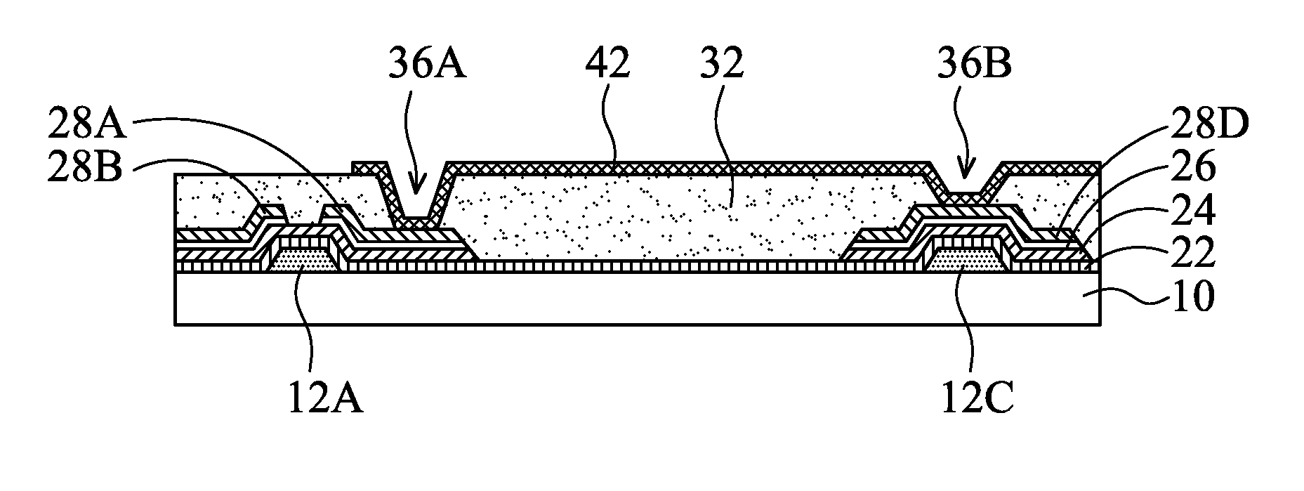
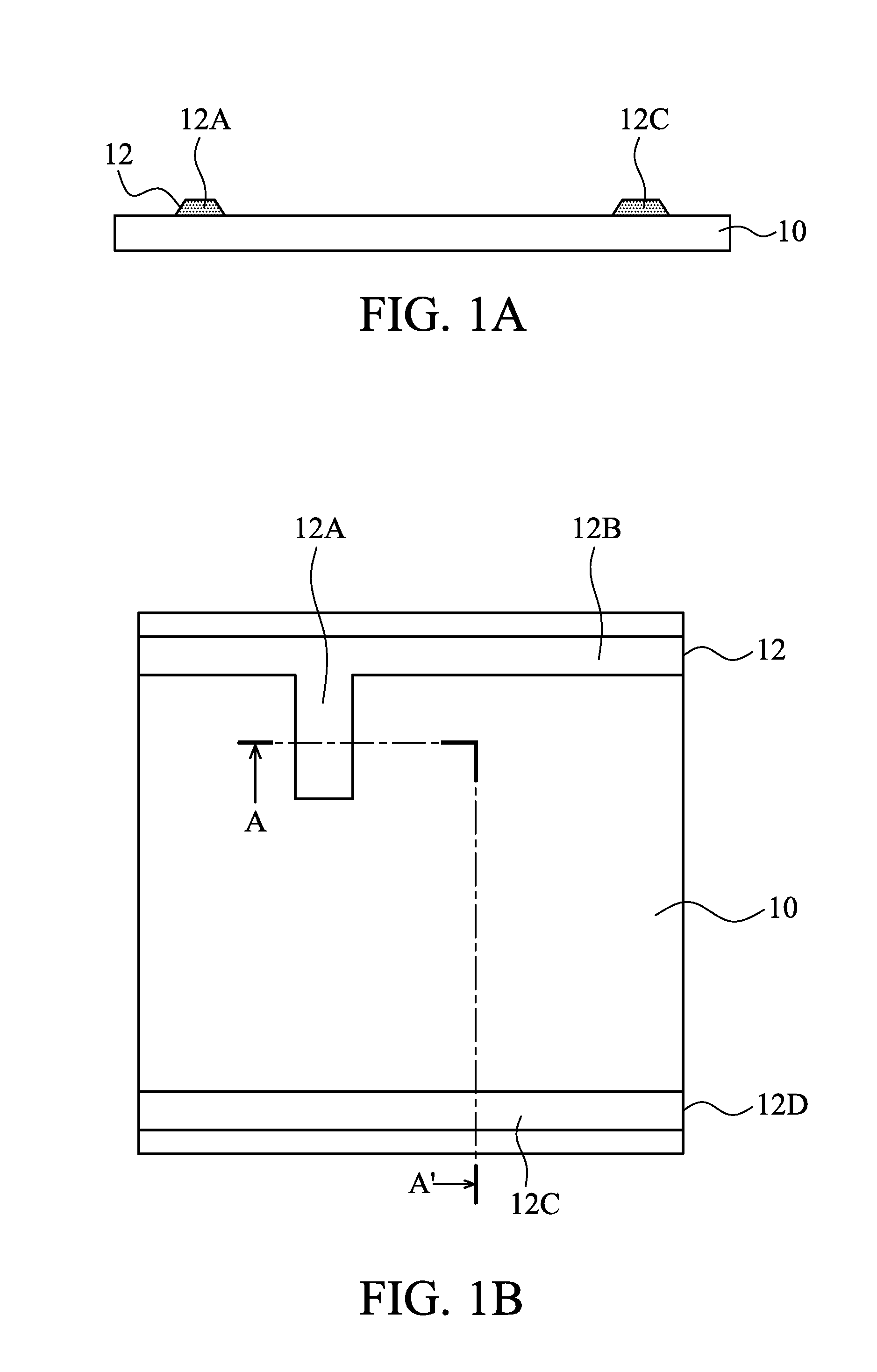
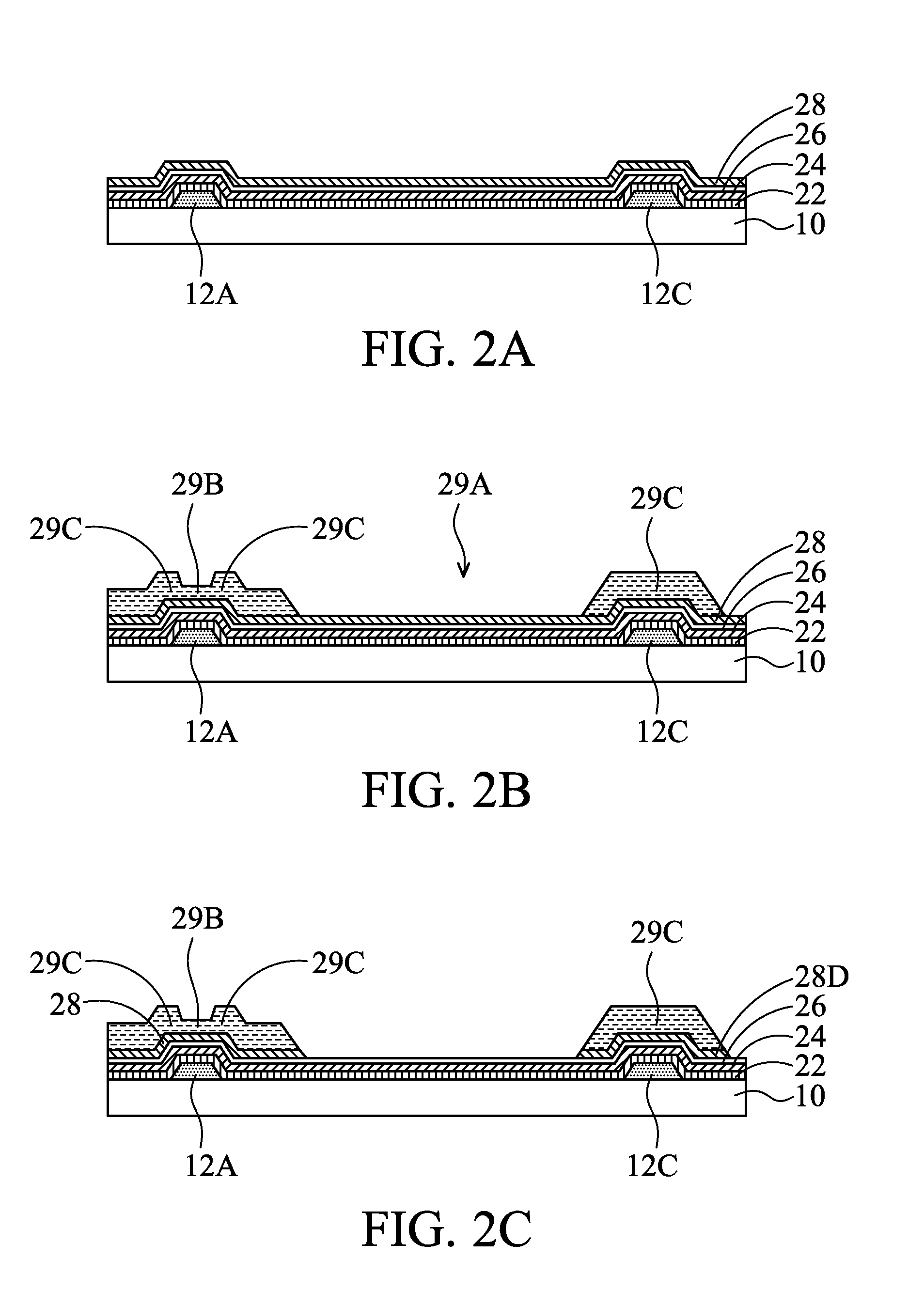
[0013]As shown in FIG. 1A, a conductive pattern 12 is formed on a substrate 10. The substrate 10 can be a rigid inorganic material, e.g. transparent material such as glass, quartz, or the likes, or an opaque material such as wafer, ceramic, or the likes. The substrate 10 can be a flexible material, such as plastic, rubber, polyester, polycarbonate, or the likes. In some embodiments, the substrate 10 of the transparent material and thin film transistor products containing the same can be applied in transmissive liquid crystal displays, reflective liquid crystal displays, or self illumination displays. In other embodiments, the substrate 10 of the opaque material or poor...


PUM


Abstract

Disclosed is a patterned photoresist layer on a passivation layer, formed by a lithography process with a multi-tone photomask, having a non-photoresist region, a thin photoresist pattern, and a thick photoresist pattern. The passivation layer corresponding to the non-photoresist region is removed, thereby forming vias to expose a part of a drain electrode in a TFT and a part of a top electrode in a storage capacitor, respectively. The thin photoresist pattern is then ashed to expose the passivation layer in a pixel region. Thereafter, a conductive layer is selectively deposited on the exposed passivation layer and on the sidewalls/bottoms of the vias. Subsequently, the remaining thick photoresist pattern is ashed.

Description

CROSS REFERENCE TO RELATED APPLICATIONS[0001]This Application claims priority of Taiwan Patent Application No. 099144151, filed on Dec. 16, 2010, the entirety of which is incorporated by reference herein.BACKGROUND OF THE INVENTION[0002]1. Field of the Invention[0003]The present invention relates to a process of manufacturing a liquid crystal display, and in particular relates to a method of manufacturing an array substrate thereof.[0004]2. Description of the Related Prior Arts[0005]General processes of forming an array substrate in a liquid crystal display need four or five lithography steps, and four or five photomasks. A lithography step with only three photomasks utilizes a lift-off process, which firstly forms a photoresist layer as a sacrificing layer of a coating film. Thereafter, the coating film is deposited on regions covered and not covered by the photoresist layer, and the substrate is dipped in a stripper. The coating film on the photoresist layer can be stripped with t...

Claims


Application Information

Patent Timeline
Patent Type & Authority Applications(United States)
IPC IPC(8): H01L21/336
CPCH01L27/1288
Inventor CHOU, CHENG-HSU
Owner INNOLUX CORP
Why Eureka
Try Eureka