In-situ low-k capping to improve integration damage resistance

a technology of low-k capping and integrated circuits, applied in the field of low-k dielectric layers for forming, can solve problems such as unwanted damag

Inactive Publication Date: 2012-06-21
APPLIED MATERIALS INC
View PDF7 Cites 341 Cited by
  • Summary
  • Abstract
  • Description
  • Claims
  • Application Information

AI Technical Summary

Problems solved by technology

However, the porous characteristics of such dielectric films lead to undesired damage after further integration steps (e.g. etching or chemical mechanical polishing (CMP)).

Method used


Image

  • In-situ low-k capping to improve integration damage resistance
  • In-situ low-k capping to improve integration damage resistance
  • In-situ low-k capping to improve integration damage resistance

Examples


examples

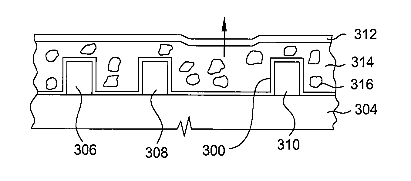
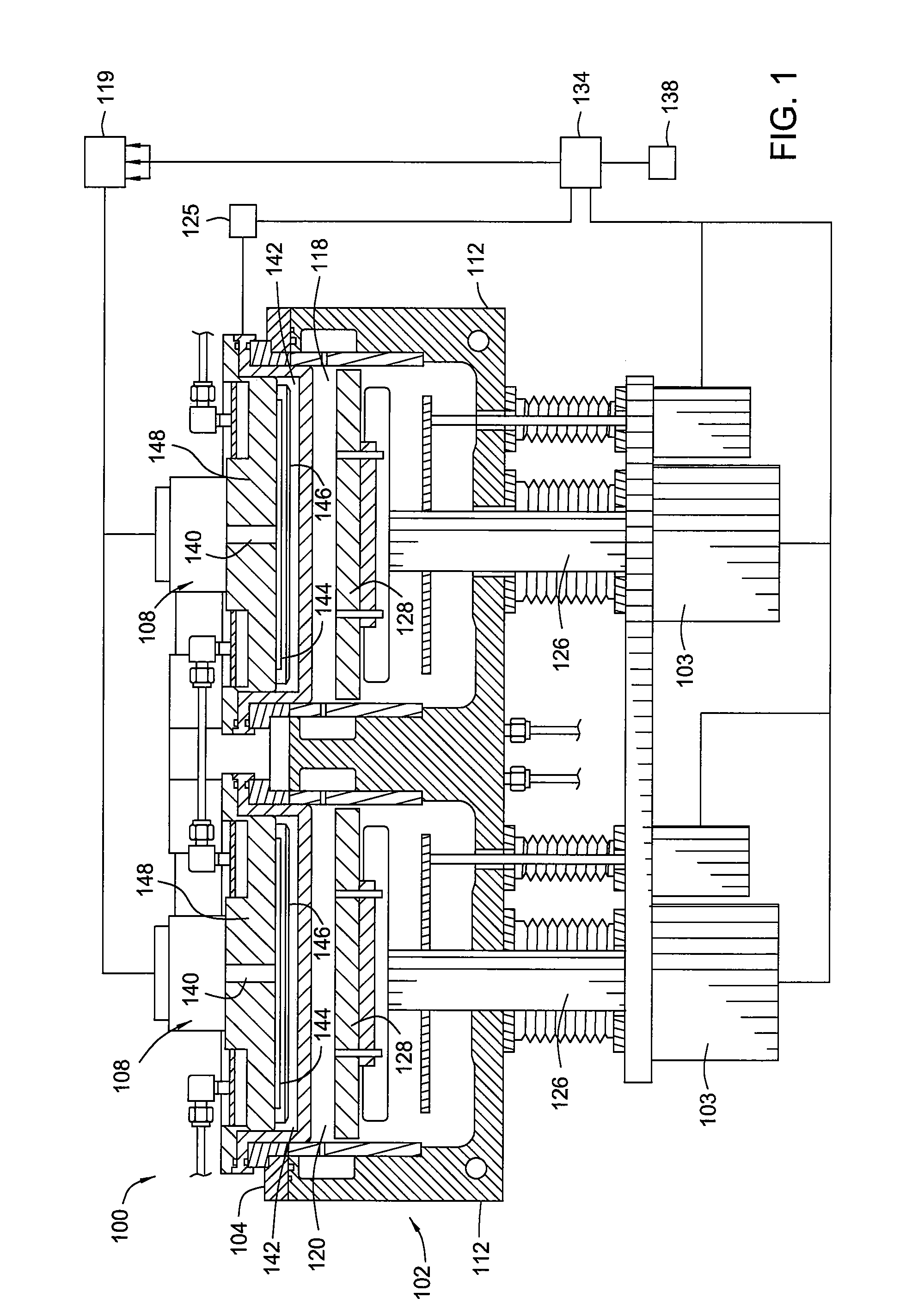
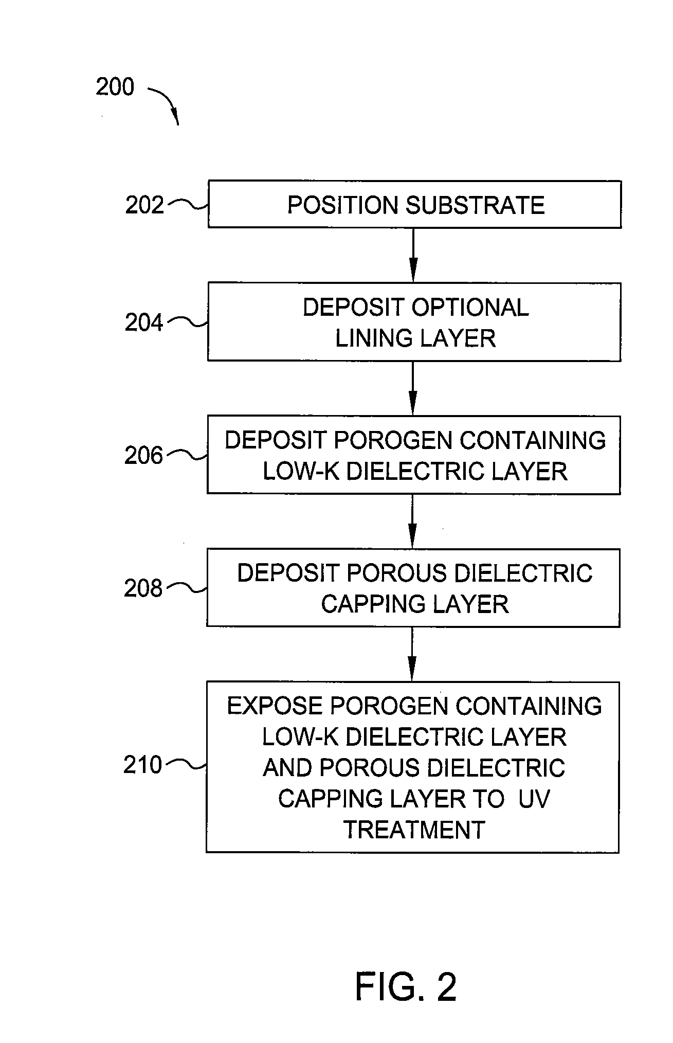
[0048]Objects and advantages of the embodiments described herein are further illustrated by the following examples. The particular materials and amounts thereof, as well as other conditions and details, recited in these examples should not be used to limit embodiments described herein. The following examples demonstrate deposition of a porous low-k dielectric layer having air-gaps with a porous dielectric capping layer deposited thereon. This example is undertaken using a PRODUCER° system, available from Applied Materials, Inc. of Santa Clara, Calif.

[0049]The porous low-k dielectric layer having air gaps and the porous dielectric capping layer were deposited in a back-to-back process using the process conditions depicted in Table II. As shown in Table II, the porous dielectric capping layer was deposited using a porogen free deposition process.

TABLE IIProcess conditions for Example IProcess Conditions for Example 1Low-k DielectricDepositionCapping LayerTemperature (° C.)260260Pressu...


PUM

PropertyMeasurementUnit
porosityaaaaaaaaaa
porosityaaaaaaaaaa
dielectric constantaaaaaaaaaa

Abstract

A method and apparatus for forming low-k dielectric layers that include air gaps is provided. In one embodiment, a method of processing a substrate is provided. The method comprises disposing a substrate within a processing region, reacting an organosilicon compound, with an oxidizing gas, and a porogen providing precursor in the presence of a plasma to deposit a porogen containing low-k dielectric layer comprising silicon, oxygen, and carbon on the substrate, depositing a porous dielectric capping layer comprising silicon, oxygen and carbon on the porogen containing low-k dielectric layer, and ultraviolet (UV) curing the porogen containing low-k dielectric layer and the porous dielectric capping layer to remove at least a portion of the porogen from the porogen containing low-k dielectric layer through the porous dielectric capping layer to convert the porogen containing low-k dielectric layer to a porous low-k dielectric layer having air gaps.

Description

CROSS-REFERENCE TO RELATED APPLICATIONS[0001]This application claims benefit of U.S. provisional patent application Ser. No. 61 / 425,020, filed Dec. 20, 2010, which is herein incorporated by reference.FIELD OF THE INVENTIONBACKGROUND OF THE INVENTION[0002]1. Field of the Invention[0003]Embodiments of the present invention generally relate to the fabrication of integrated circuits. More particularly, embodiments of the present invention relate to methods for forming low-k dielectric layers that include air gaps.[0004]2. Description of the Related Art[0005]Integrated circuit geometries have dramatically decreased in size since such devices were first introduced several decades ago. Since then, integrated circuits have generally followed the two year / half-size rule (often called Moore's Law), which means that the number of devices on a chip doubles every two years. Today's fabrication facilities are routinely producing devices having 0.1 micron feature sizes, and tomorrow's facilities s...

Claims


Application Information

Patent Timeline
Patent Type & Authority Applications(United States)
IPC IPC(8): H01L21/3105
CPCH01L21/02126H01L21/02203H01L21/02214H01L21/02216H01L2221/1047H01L21/02348H01L21/02362H01L21/7682H01L21/76829H01L21/02274H01L21/205H01L21/31H01L21/3105
Inventor YIM, KANG SUBXU, JINNGO, SUREDEMOS, ALEXANDROS T.
Owner APPLIED MATERIALS INC
Why Eureka
Try Eureka