
Plasma processing apparatus and substrate processing method

a processing apparatus and substrate technology, applied in the direction of plasma technique, chemical vapor deposition coating, coating, etc., can solve the problems of high equipment cost, non-uniform plasma process on the surface of the processing target substrate, and deviation reduction, so as to prevent non-uniform distribution

Active Publication Date: 2012-06-28
TOKYO ELECTRON LTD
View PDF6 Cites 186 Cited by
  • Summary
  • Abstract
  • Description
  • Claims
  • Application Information

AI Technical Summary

Benefits of technology

[0028]In accordance with a plasma processing apparatus of an illustrative embodiment, even if centers of an inner conductor and an outer conductor of a coaxial waveguide are deviated when the coaxial waveguide is manufactured, a distance between a part of an outer surface of the inner conductor and a facing member facing the part of the outer surface of the inner conductor in a radial direction can be adjusted by a distance varying device for varying the distance between the part of the outer surface of the inner conductor and the facing member facing the part of the outer surface of the inner conductor. Accordingly, microwave can be non-uniformly (asymmetrically) propagated within the coaxial waveguide in a circumferential direction. In this way, it may be possible to prevent non-uniform distribution of an electromagnetic field formed at a dielectric plate in the circumferential direction, which is caused by a deviation between the centers of the inner conductor and the outer conductor. As a result, plasma can be uniformly generated on a lower surface of the dielectric plate within a processing chamber. In such a case, it may be also possible to prevent non-uniform distribution of the electromagnetic field in the circumferential direction, which is caused by the error in mounting a wavelength shortening plate. Consequently, a process can be performed uniformly within a surface of a processing target substrate.
[0029]Further, in accordance with the substrate processing method as stated above, it is possible to perform the process uniformly within the surface of the processing target substrate.

Problems solved by technology

Such a non-uniform distribution of the electromagnetic field may cause a non-uniform distribution of plasma generated within the processing chamber in a circumferential direction, resulting in non-uniformity of the plasma process within the surface of the processing target substrate.
Here, when assembling the coaxial waveguide 107, it is very difficult to reduce the deviation between the centers of the inner conductor 108 and the outer conductor 109 so as not to cause the non-uniformity of plasma distribution, and thus, a high equipment cost may be required.
Furthermore, the same problems may also be caused when positioning the wavelength shortening plate and the dielectric plate.

Method used


Image

  • Plasma processing apparatus and substrate processing method
  • Plasma processing apparatus and substrate processing method
  • Plasma processing apparatus and substrate processing method

Examples


Embodiment Construction

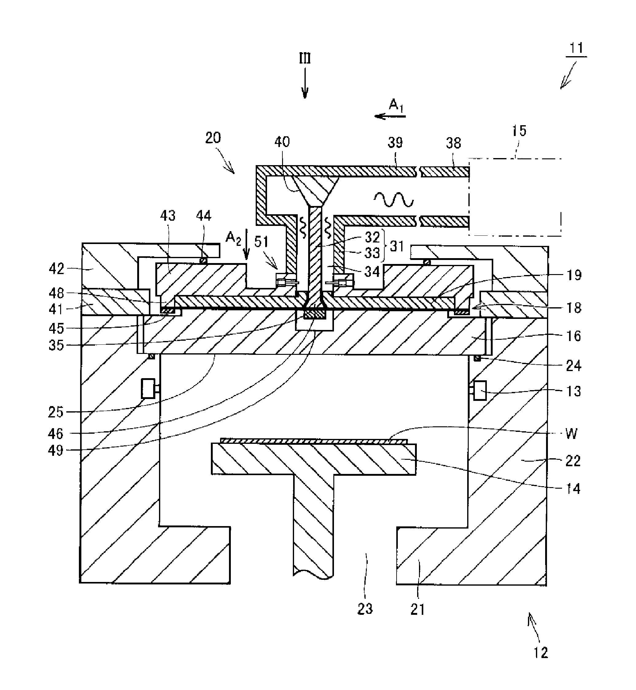
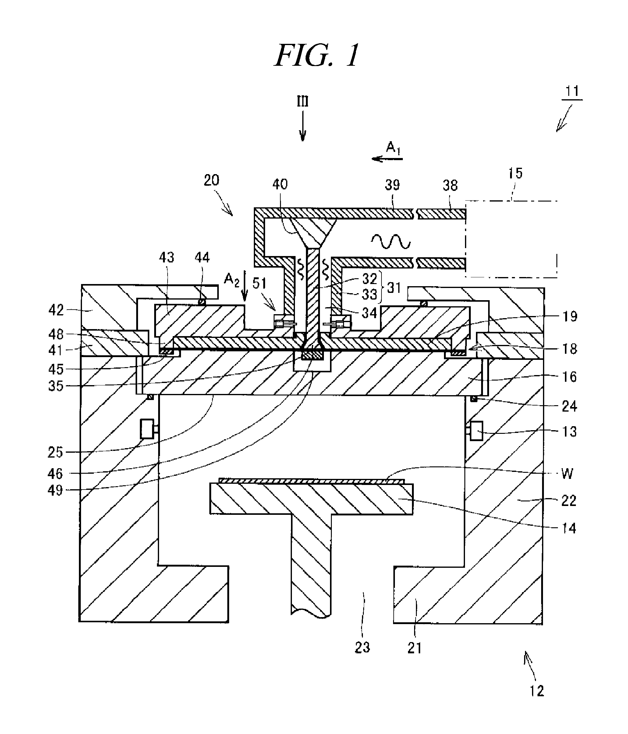
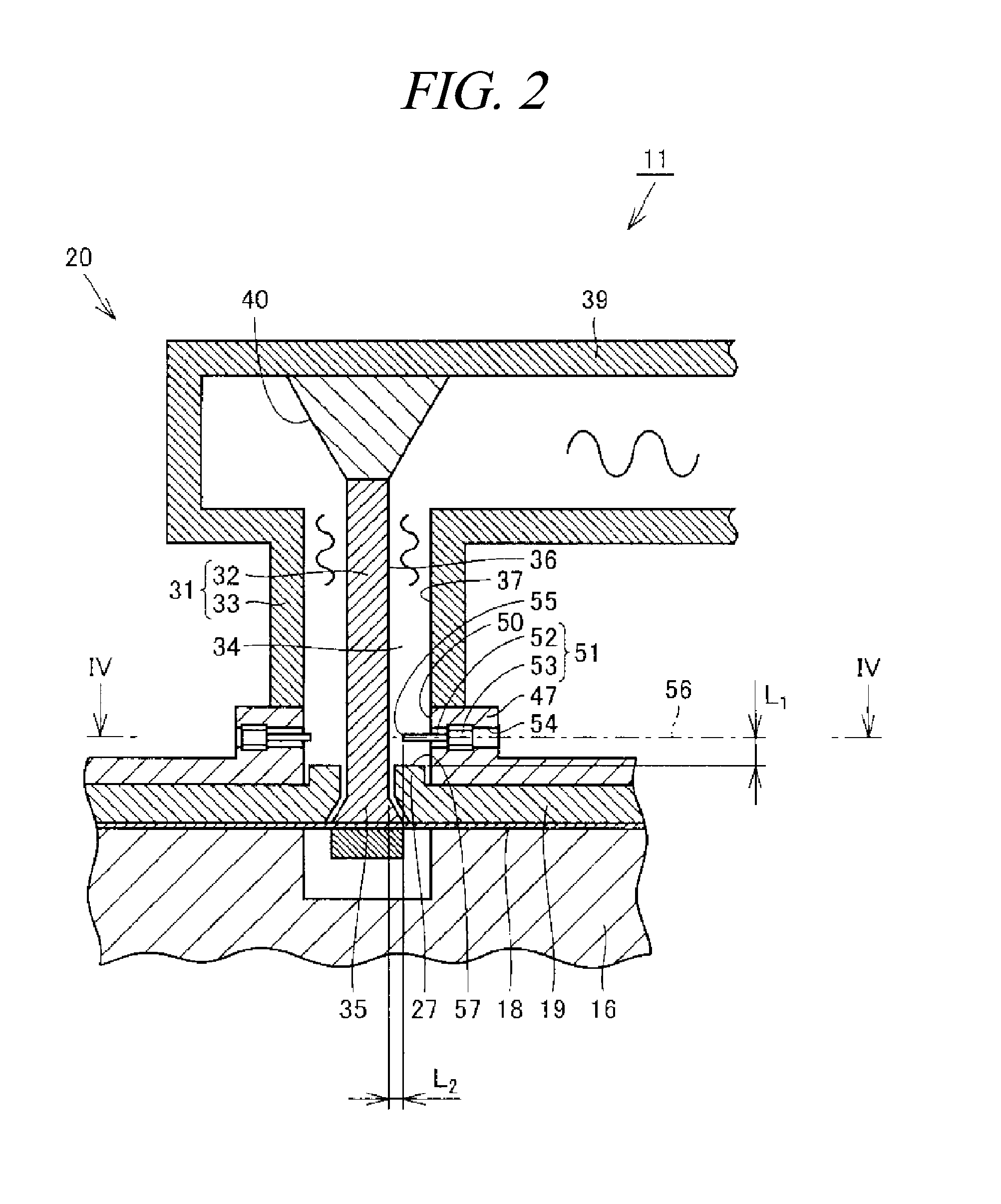
[0048]Hereinafter, illustrative embodiments will be described with reference to the accompanying drawings. FIG. 1 is a schematic cross sectional view illustrating major components of a plasma processing apparatus in accordance with an illustrative embodiment. FIG. 2 provides an enlarged schematic cross sectional view illustrating a coaxial waveguide and the vicinity thereof included in the plasma processing apparatus of FIG. 1. FIG. 3 is a diagram illustrating a slot antenna plate included in the plasma processing apparatus of FIG. 1, when viewed from a direction of an arrow III of FIG. 1. FIG. 4 is a cross sectional view of the coaxial waveguide included in the plasma processing apparatus of FIG. 1, taken along a line IV-IV of FIG. 2. In FIGS. 1 and 2, a vertical direction of the drawings corresponds to a vertical direction of the plasma processing apparatus. Further, the term ‘radial direction’ used in the entire specification refers to a direction from an inner conductor toward a...


PUM

PropertyMeasurementUnit
Distanceaaaaaaaaaa
Distanceaaaaaaaaaa
Dielectric polarization enthalpyaaaaaaaaaa

Abstract

A microwave supply unit 20 of a plasma processing apparatus 11 includes a stub member 51 configured to be extensible from the outer conductor 33 toward the inner conductor 32. The stub member 51 serves as a distance varying device for varying a distance in the radial direction between a part of the outer surface 36 of the inner conductor 32 and a facing member facing the part of the outer surface of the inner conductor 32 in the radial direction, i.e., the cooling plate protrusion 47. The stub member 51 includes a rod-shaped member 52 supported at the outer conductor 33 and configured to be extended in the radial direction; and a screw 53 as a moving distance adjusting member for adjusting a moving distance of the rod-shaped member 52 in the radial direction.

Description

TECHNICAL FIELD[0001]The present disclosure relates to a plasma processing apparatus and a substrate processing method; and, more particularly, to a plasma processing apparatus using microwave as a plasma source and a substrate processing method that is performed by the plasma processing apparatus.BACKGROUND ART[0002]A semiconductor device such as a LSI (Large Scale Integrated circuit) is manufactured by performing various processes such as an etching process, a CVD (Chemical Vapor Deposition) process, a sputtering process on a semiconductor substrate. A processing method using plasma as an energy source, i.e., a plasma etching process, a plasma CVD process or a plasma sputtering process may be used to perform the etching process, the CVD process or the sputtering process.[0003]Here, a microwave plasma processing apparatus using microwave for generating plasma is described in Japanese Patent Laid-open Publication No. 2006-179477 (Patent Document 1). In Patent Document 1, a dummy loa...

Claims


Application Information

Patent Timeline
IPC IPC(8): B44C1/22H01L21/3065H05H1/46C23C16/511
CPCC23C16/511H01J37/32192H05H2001/463H01J37/32229H05H1/46H01J37/3222H05H1/463H05H1/4622C23C16/455H01J37/3244
Inventor ISHIBASHI, KIYOTAKAMORITA, OSAMU
Owner TOKYO ELECTRON LTD
Features
  • Generate Ideas
  • Intellectual Property
  • Life Sciences
  • Materials
  • Tech Scout
  • Unparalleled Data Quality
  • Higher Quality Content
  • 60% Fewer Hallucinations
Learn More