Gate drive circuit, display substrate having the same and method of manufacturing the display substrate

Active Publication Date: 2012-06-28
SAMSUNG DISPLAY CO LTD
View PDF13 Cites 27 Cited by
  • Summary
  • Abstract
  • Description
  • Claims
  • Application Information

AI Technical Summary

Benefits of technology

[0034]According to some example embodiments, a capacitor part is formed in a parallel structure, so that an integrated size of a gate drive circuit may be decreased. Moreover, a coupling capacitance, which is generated between an el

Problems solved by technology

Thus, manufacturing costs of the LCD panel may be increased.
However, if a width of the gate drive circuit is increased when the size of the glass substrate is fixed, the number of

Method used


Image

  • Gate drive circuit, display substrate having the same and method of manufacturing the display substrate
  • Gate drive circuit, display substrate having the same and method of manufacturing the display substrate
  • Gate drive circuit, display substrate having the same and method of manufacturing the display substrate

Examples


Embodiment Construction

[0047]Hereinafter, the claimed subject matter will be explained in detail with reference to the accompanying drawings.

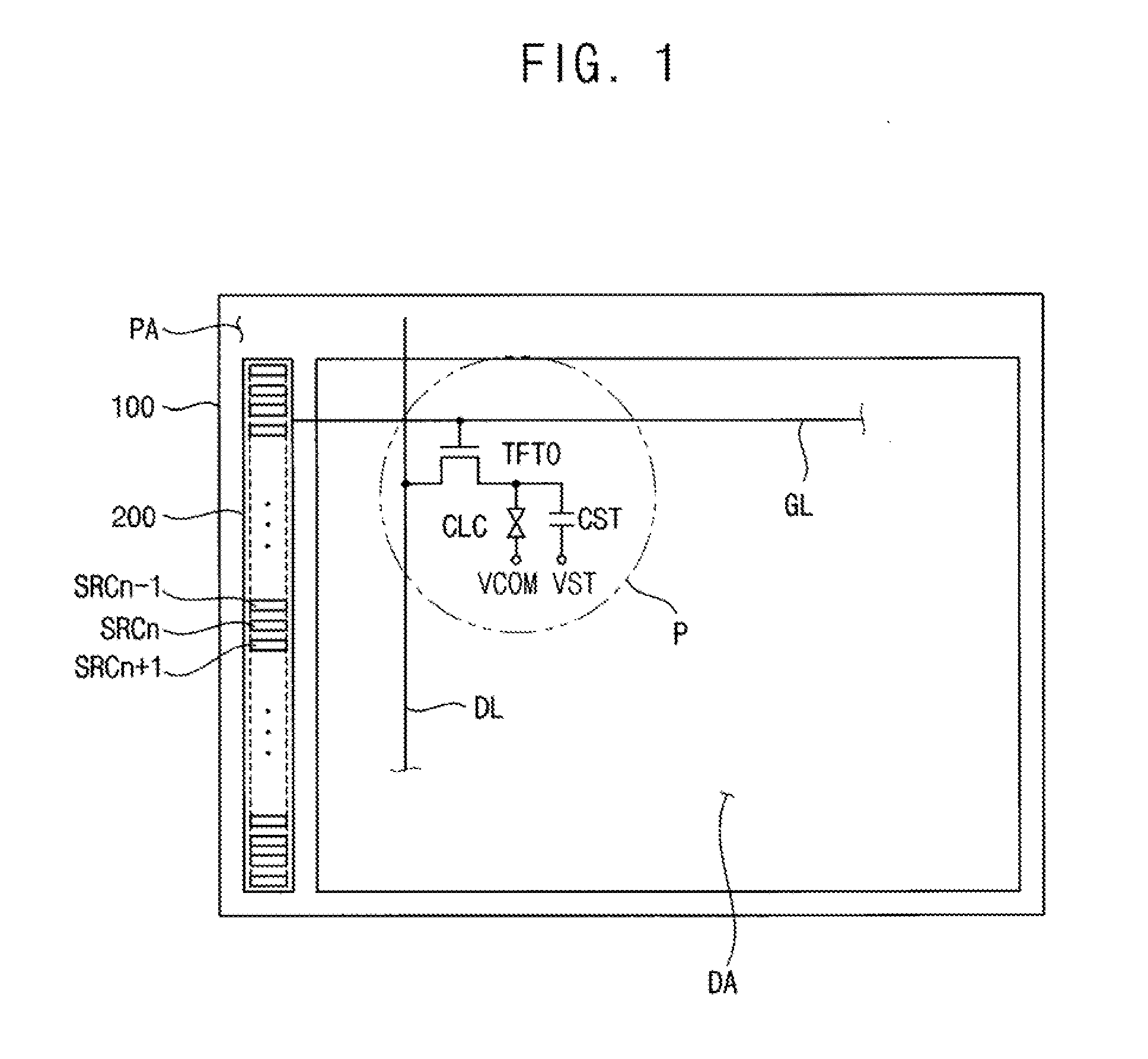
[0048]FIG. 1 is a plan view schematically showing a display substrate according to an exemplary embodiment.

[0049]Referring to FIG. 1, the display substrate includes a base substrate 100 including a display area DA and a peripheral area PA surrounding the display area DA, a pixel part P formed on the display area DA and a gate drive circuit 200 formed on the peripheral area PA.

[0050]The pixel part P includes a plurality of pixel transistors TFTO electrically connected to gate lines GL and data lines DL, a plurality of liquid crystal capacitors CLC electrically connected to the pixel transistors TFT0, and a plurality of storage capacitors CST connected to the liquid crystal capacitors CLC in parallel.

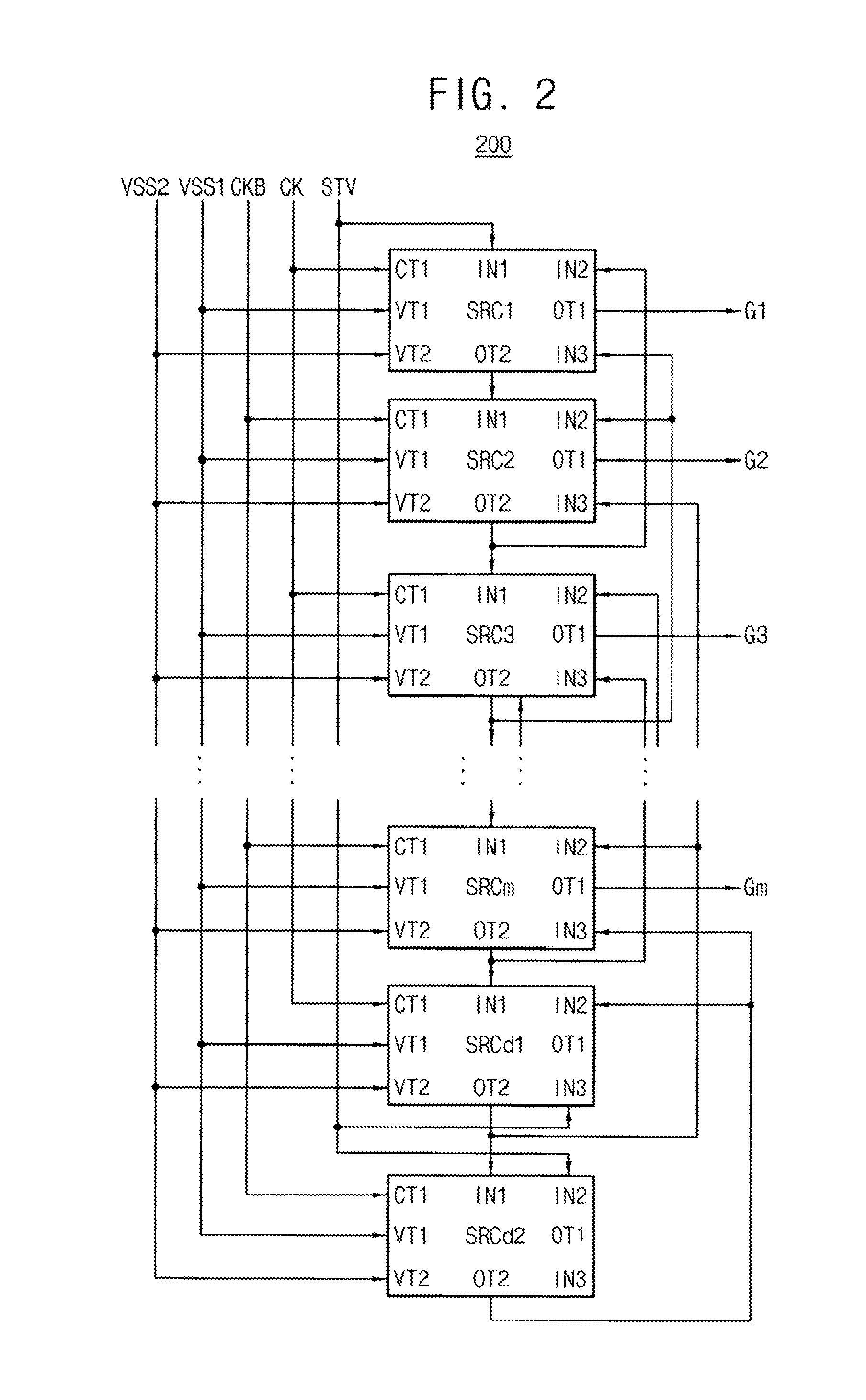
[0051]The gate drive circuit 200 includes a shift register sequentially outputting gate signals of a high level to the gate lines GL. The shift register includes a plurali...


PUM


Abstract

A gate drive circuit includes plural stages connected together one after each other. Each of the plural stages includes a circuit transistor, a capacitor part, a first connection part and a second connection part. The circuit transistor outputs the gate signal through a source electrode in response to a control signal applied through a gate electrode. The capacitor part includes a first electrode, a second electrode formed on the first electrode, and a third electrode formed on the second electrode. The first connection part electrically connects the gate electrode of the circuit transistor and the second electrode of the capacitor part. The second connection part electrically connects the source electrode of the circuit transistor and the first electrode of the capacitor part. Thus, an integrated size of a gate drive circuit may be decreased, and a reliability of a gate drive circuit may be enhanced.

Description

PRIORITY STATEMENT[0001]This application claims priority under 35 U.S.C. §119 to Korean Patent Application No. 10-2010-0135278, filed on Dec. 27, 2010 in the Korean Intellectual Property Office (KIPO), the contents of which are herein incorporated by reference in their entirety.BACKGROUND[0002]1. Field of the Invention[0003]Example embodiments of the claimed subject matter relate to a gate drive circuit, a display substrate having the gate drive circuit, and a method of manufacturing the display substrate. More particularly, example embodiments of the relate to a gate drive circuit used to a liquid crystal display (“LCD”) device, a display substrate having the gate drive circuit, and a method of manufacturing the display substrate.[0004]2. Description of the Related Art[0005]In general, an LCD device includes an LCD panel displaying images using light transmittance of a liquid crystal and a backlight assembly disposed below the LCD panel to provide the LCD panel with lights.[0006]Th...

Claims


Application Information

Patent Timeline
IPC IPC(8): H03K3/00H01L33/08
CPCG09G3/3611H01L29/41733H01L27/1259H01L27/1255G02F1/1343
Inventor KOO, BON-YONGKIM, SUNG-MANLEE, JAE-HOON
Owner SAMSUNG DISPLAY CO LTD
Why Eureka
Try Eureka