Vertical transistor manufacturing method and vertical transistor

a manufacturing method and transistor technology, applied in the field of vertical transistors, can solve the problems of deterioration of the breakdown characteristics of the vertical transistor, difficult growth of a high integrity dielectric layer, etc., and achieve the effect of improving the breakdown characteristics

Inactive Publication Date: 2012-07-05
NXP BV
View PDF2 Cites 16 Cited by
  • Summary
  • Abstract
  • Description
  • Claims
  • Application Information

AI Technical Summary

Benefits of technology

[0008]The present invention seeks to provide a method of manufacturing a vertical transistor having improved breakdown characteristics.
[0009]The present invention further seeks to provide a vertical transistor having improved breakdown characteristics.

Problems solved by technology

A problem that in particular arises when the shield electrode is implemented as a doped polysilicon electrode is that the growth of a high integrity dielectric layer and in particular an oxide layer over such a material is notoriously difficult as an oxide layer grown on a (doped) polysilicon surface has a lower field to breakdown than an oxide layer grown on a monocrystalline silicon surface.
This has the additional problem that upon formation of the gate oxide 15 in the top portion of the trench 23, a weak spot is formed at the interface between the gate oxide 15 and the gate oxide 9, which can cause a deterioration of the breakdown characteristics of the vertical transistor.

Method used


Image

  • Vertical transistor manufacturing method and vertical transistor
  • Vertical transistor manufacturing method and vertical transistor
  • Vertical transistor manufacturing method and vertical transistor

Examples


Embodiment Construction

[0021]Embodiments of the invention are described in more detail and by way of non-limiting examples with reference to the accompanying drawings, wherein

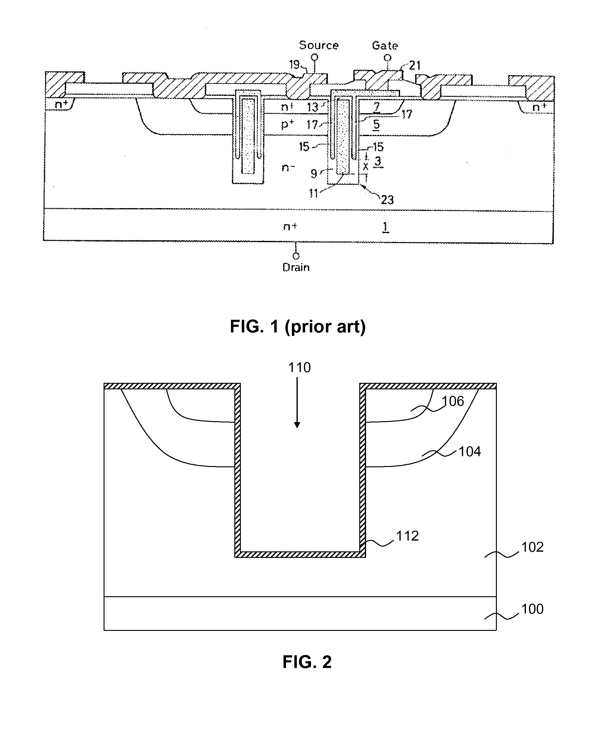
[0022]FIG. 1 schematically depicts a prior art vertical MOS transistor;

[0023]FIG. 2-10 schematically depict various steps of an embodiment of the method of the present invention; and

[0024]FIG. 11 is a scanning electron microscope (SEM) image of a device comprising vertical transistors manufactured in accordance with an embodiment of the method of the present invention.

DETAILED DESCRIPTION OF THE DRAWINGS

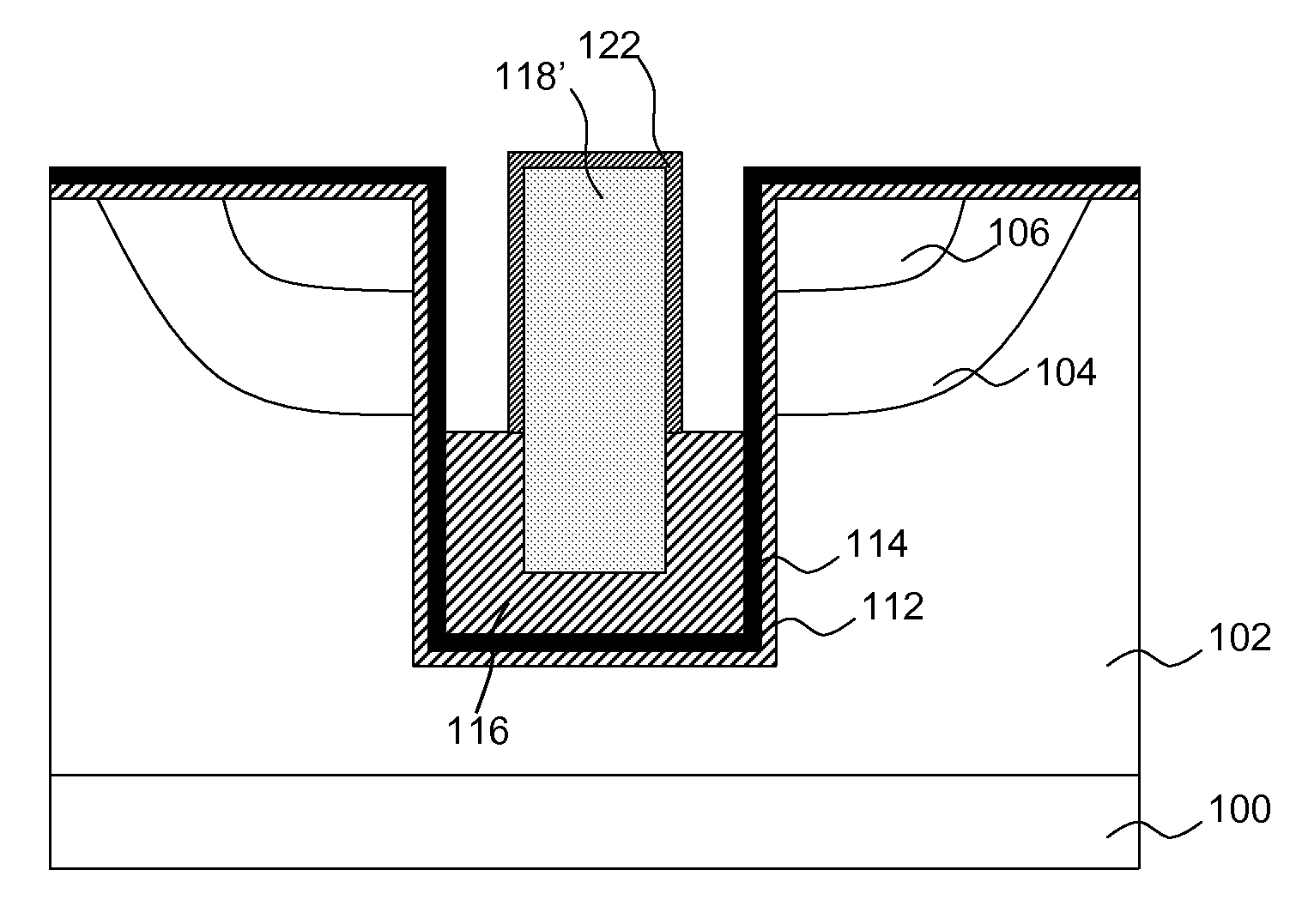
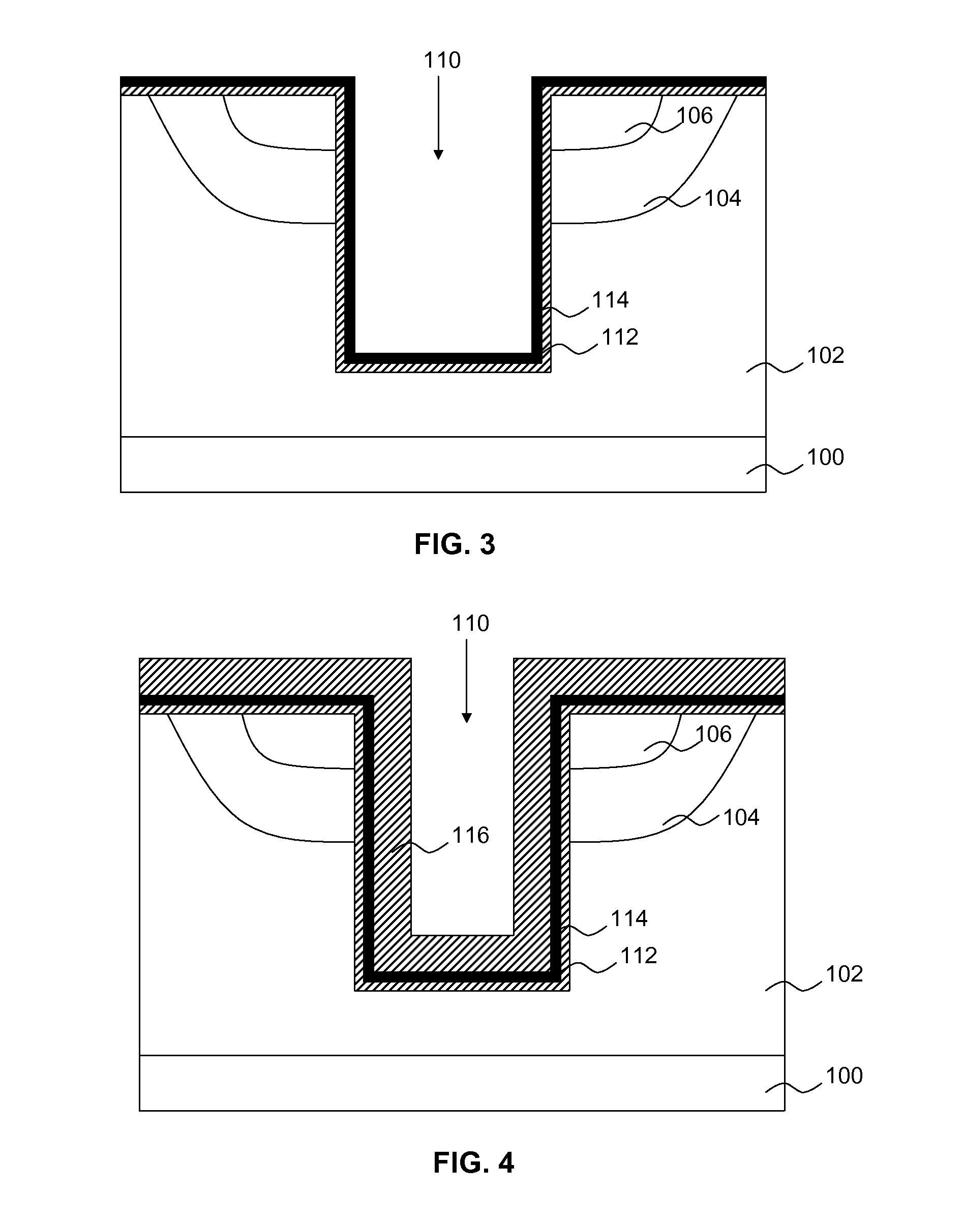
[0025]It should be understood that the Figures are merely schematic and are not drawn to scale. It should also be understood that the same reference numerals are used throughout the Figures to indicate the same or similar parts.

[0026]FIGS. 2-10 schematically depict the main steps of an example embodiment of the method of the present invention for manufacturing a vertical MOS transistor, also referred to as a trench MOS transistor. It ...


PUM


Abstract

A method is disclosed of manufacturing a vertical transistor which comprises providing a substrate including a vertical stack of regions including a source region separated from a drain region by a channel region; forming a trench in said substrate, said trench at least partially extending into said vertical stack of regions; lining said trench with a stack comprising a gate dielectric liner, an etch protection layer and a further insulating layer; filling the remainder of the trench with a shield electrode material; exposing a top portion of the shield electrode material by removing the further insulating layer to a first depth in said trench; forming a inter electrode dielectric on the exposed shield electrode material; removing the etch protection layer to the first depth from said trench; and forming a gate electrode in said trench between the inter electrode dielectric liner and the exposed portion of the gate dielectric liner.

Description

FIELD OF THE INVENTION[0001]The present invention relates to a vertical transistor comprising a substrate including a vertical stack of regions including a source region separated from a drain region by a channel region and a trench lined with a gate dielectric liner, said trench at least partially extending through said vertical stack of regions, wherein said trench comprises a shield electrode and a gate electrode surrounding an upper portion of the shield electrode.[0002]The present invention further relates to a method of manufacturing such a vertical transistor.BACKGROUND OF THE INVENTION[0003]Vertical transistors, e.g. trench-MOS (metal oxide semiconductor) transistors are promising devices to allow for the further increase of the device density in a semiconductor chip. In order to improve the characteristics of such vertical transistors, architectures have been proposed in which in addition to the vertical gate electrode, a shield electrode is provided, as the presence of the...

Claims


Application Information

Patent Timeline
Patent Type & Authority Applications(United States)
IPC IPC(8): H01L29/78H01L21/336
CPCH01L29/407H01L29/42368H01L29/42376H01L29/7813H01L29/518H01L29/66734H01L29/513
Inventor JIN, MINGHAOCALTON, DAVID WILLIAMKERSHAW, NICKROGERS, CHRIS
Owner NXP BV
Why Eureka
Try Eureka