Semiconductor memory device and method of operating the same

Active Publication Date: 2012-07-05
SK HYNIX INC
View PDF2 Cites 11 Cited by
  • Summary
  • Abstract
  • Description
  • Claims
  • Application Information

AI Technical Summary

Benefits of technology

[0007]According to exemplary embodiments, in a read operation for an even page, a shift of the threshold voltages of even memory cells due to a program interference phenomenon is predicted by detecting the threshold voltages of the even memory cells and odd memory cells on both sides of each of the even memory cells. A read operation condition for the even memory cells is controlled according to the result of the prediction. Accordingly, reliability of output data can be improved.

Problems solved by technology

Since the even page program operation is performed earlier than the odd page program operation, the threshold voltages of memory cells included in the even pages are relatively greatly shifted owing to the program interference phenomenon.
Accordingly, a threshold voltage distribution of the memory cells may be widened, and an error may occur in an operation of reading data.

Method used


Image

  • Semiconductor memory device and method of operating the same
  • Semiconductor memory device and method of operating the same
  • Semiconductor memory device and method of operating the same

Examples


Embodiment Construction

[0022]Hereinafter, some exemplary embodiments of the present disclosure will be described in detail with reference to the accompanying drawings. The figures are provided to allow those having ordinary skill in the art to understand the scope of the exemplary embodiments of the disclosure.

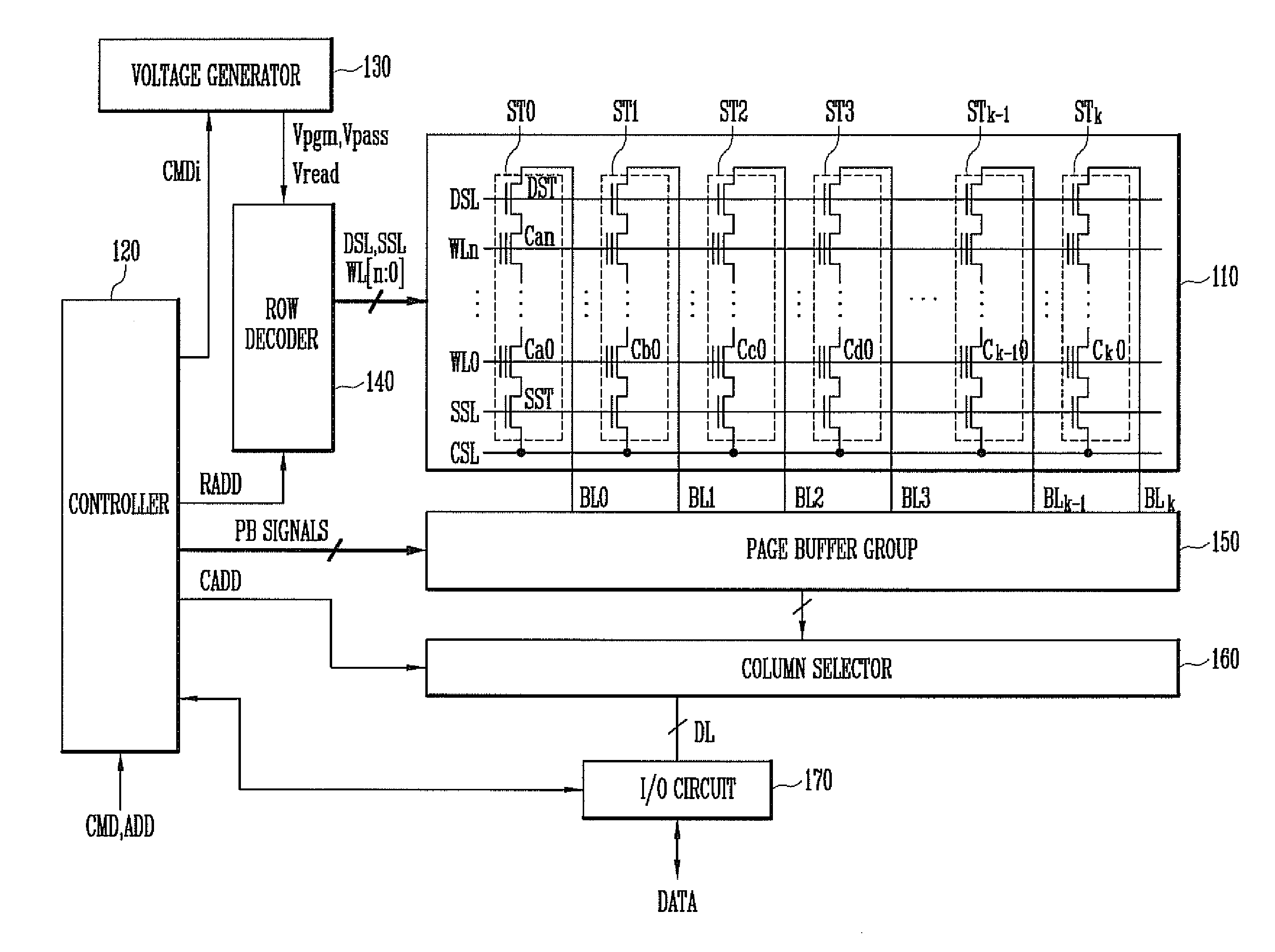
[0023]FIG. 1 is a circuit diagram of a semiconductor memory device according to an exemplary embodiment of this disclosure.

[0024]Referring to FIG. 1, the semiconductor memory device according to the exemplary embodiment of this disclosure includes a memory cell array 110, an operation circuit group (130, 140, 150, 160, 170) for performing a program operation or a read operation for the memory cells of the memory cell array 110, and a controller 120 for controlling the operation circuit group (130, 140, 150, 160, 170) so that the program operation or the read operation of the memory cells is performed.

[0025]In a NAND flash memory device, the operation circuit group includes a voltage supply circuit (...


PUM


Abstract

A semiconductor memory device according to an aspect of the present disclosure includes a first page buffer coupled to a first even bit line and a first odd bit line, a second page buffer coupled to a second even bit line and a second odd bit line, and a controller configured to control the first and the second page buffers so that the second page buffer sets the second even bit line in a floating state such that the voltage of the second even bit line is changed according to a shift in the voltage of the first odd bit line, when a read operation for memory cells coupled to the first odd bit line is performed, and the second page buffer stores data corresponding to the level of threshold voltages of the memory cells by detecting a shift in the voltage of the second even bit line.

Description

CROSS-REFERENCE TO RELATED APPLICATION[0001]Priority to Korean patent application number 10-2010-0139171 filed on Dec. 30, 2010, the entire disclosure of which is incorporated by reference herein, is claimed.BACKGROUND[0002]Exemplary embodiments relate to a semiconductor memory device and a method of operating the same and, more particularly, to a nonvolatile memory device and a method of operating the same.[0003]A NAND flash memory device is a representative nonvolatile memory device. The memory cell array of the NAND flash memory device includes a plurality of memory blocks. Each of the memory blocks includes a plurality of memory strings coupled between bit lines and a common source line. Each of the memory strings includes a drain select transistor, memory cells, and a source select transistor coupled in series between each bit line and the common source line. The gates of the drain select transistors are coupled to a drain select line, the control gates of the memory cells are ...

Claims


Application Information

Patent Timeline
IPC IPC(8): G11C16/26G11C16/06
CPCG11C11/5642G11C16/0483G11C16/3404G11C16/26G11C16/06
Inventor AHN, SUNG HOON
Owner SK HYNIX INC
Why Eureka
Try Eureka