
Method of manufacturing an integrated circuit device

Inactive Publication Date: 2012-07-12
SAMSUNG ELECTRONICS CO LTD
View PDF21 Cites 7 Cited by
  • Summary
  • Abstract
  • Description
  • Claims
  • Application Information

AI Technical Summary

Benefits of technology

[0012]Example embodiments of the present inventive concept provide an integrated circuit device in which a contact resistance of a resistor is minimized.
[0034]The resistor pattern for applying a reference voltage to cell transistors may be provided with the bulk device isolation layer in such a configuration that the resistor body is arranged in the recess of the bulk device isolation layer and the connector is arranged around the recess of the bulk device isolation layer, so that the resistor pattern may have a stepped portion between the resistor body and the connector. Particularly, the metal silicide may be arranged at the upper portion of the connector of the resistor pattern. Thus, a contact resistance Rc between the connector and the resistor interconnection may be sufficiently reduced without any deterioration of a sheet resistance Rs of the resistor body. Accordingly, the electrical resistance of the resistor pattern may be reduced and become stable, and thus the reference voltage may be applied to the cell transistors with high reliability.

Problems solved by technology

In conventional integrated circuit devices, the resistor has an electric resistance greater than that of wiring structures and thus low-resistive materials for the wiring structure are insufficient for the resistor.
However, when polysilicon of the resistor and the metal of the connector make direct contact with each other, a plurality of voids is generated at the boundary area of the connector and the resistor due to the silicidation process of the polysilicon and the metal.
Thus, the large resistance variation of the resistor necessarily leads to an unstable operation of the reference cell operator, thereby severely deteriorating the reliability of the flash memory device.
Recently, the resistance variation of the resistor is tend to increase due to the reduction of critical dimension (CD) of semiconductor chips and thus the operation reliability of the integrated circuit devices is tend to be deteriorated.

Method used


Image

  • Method of manufacturing an integrated circuit device
  • Method of manufacturing an integrated circuit device
  • Method of manufacturing an integrated circuit device

Examples


Embodiment Construction

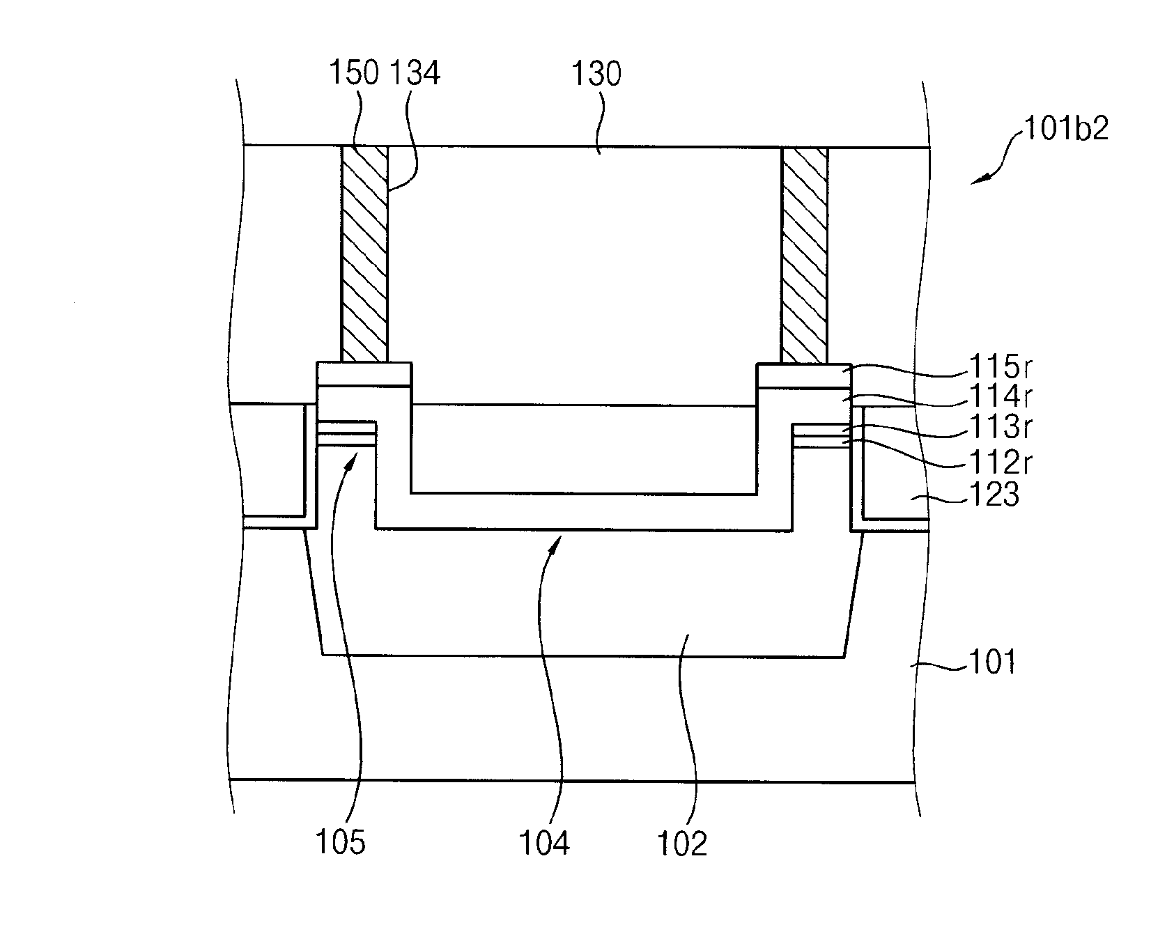
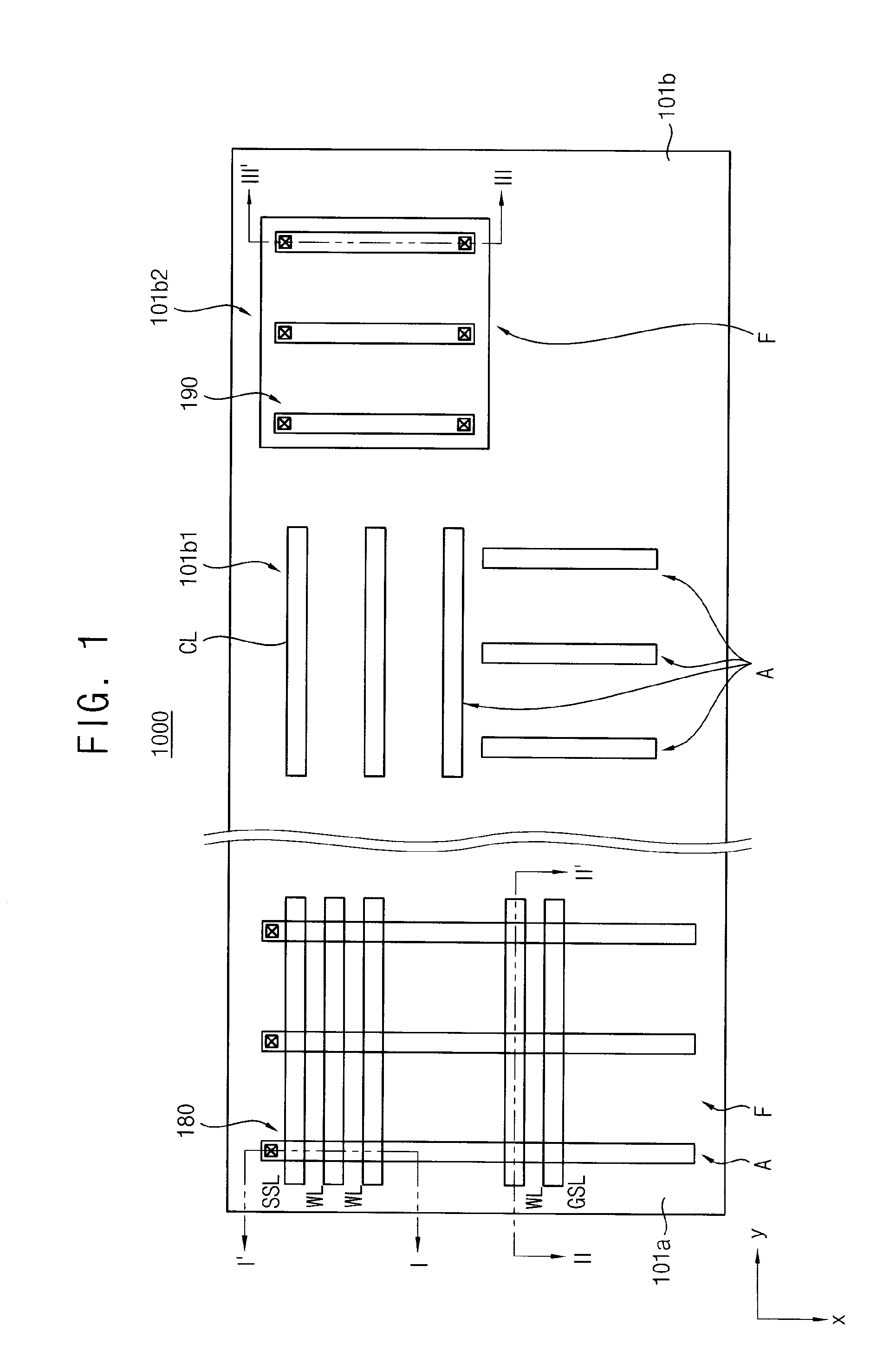
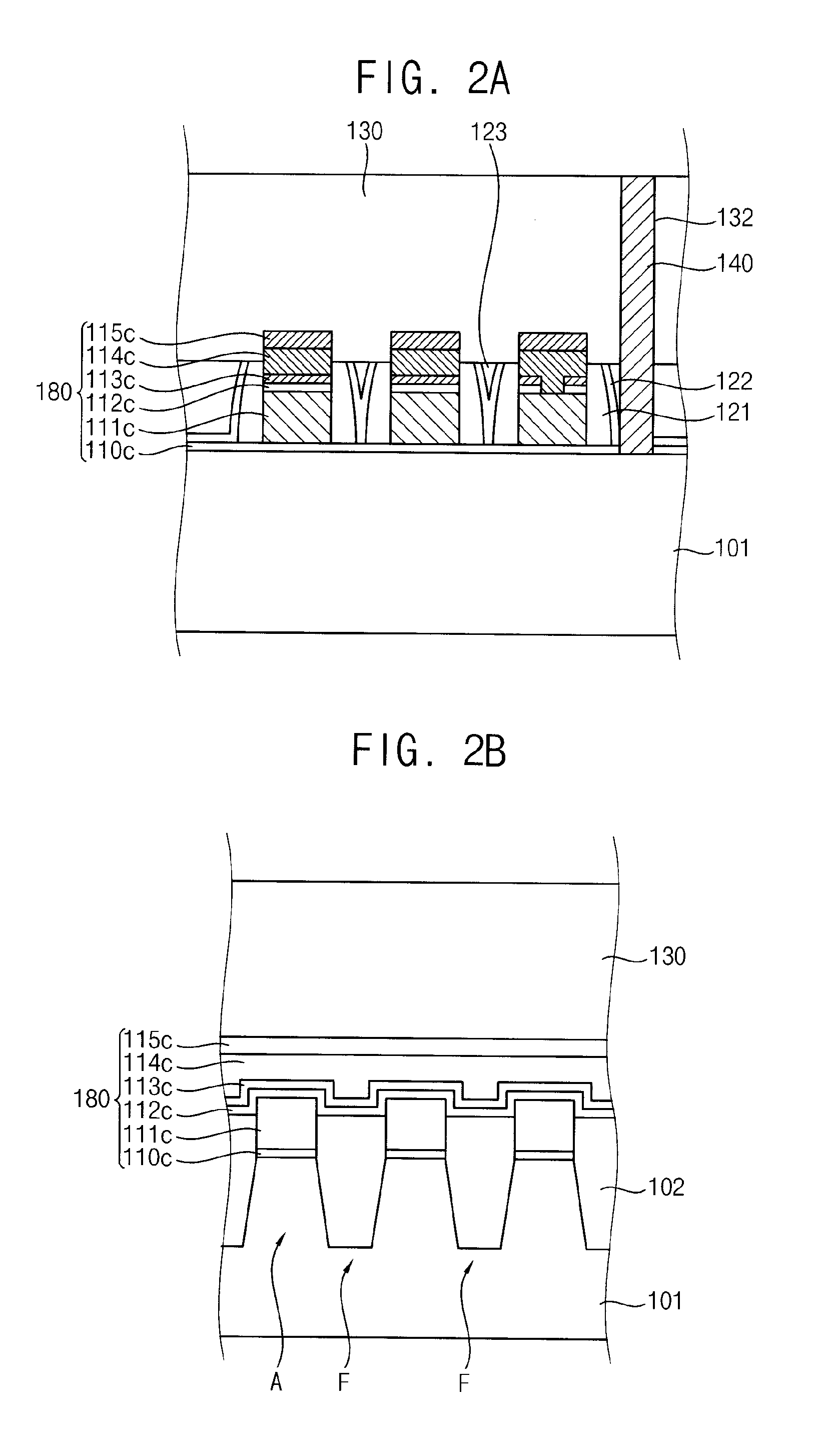
[0051]Reference will now be made in detail to the embodiments of the present general inventive concept, examples of which are illustrated in the accompanying drawings, wherein like reference numerals refer to the like elements throughout. The embodiments are described below in order to explain the present general inventive concept while referring to the figures. The present invention may, however, be embodied in many different forms and should not be construed as limited to the example embodiments set forth herein. Rather, these example embodiments are provided so that this disclosure will be thorough and complete, and will fully convey the scope of the present invention to those skilled in the art. In the drawings, the sizes and relative sizes of layers and regions may be exaggerated for clarity.

[0052]It will be understood that when an element or layer is referred to as being “on,”“connected to” or “coupled to” another element or layer, it can be directly on, connected or coupled t...


PUM


Abstract

In an integrated circuit device and method of manufacturing the same, a resistor pattern is positioned on a device isolation layer of a substrate. The resistor pattern includes a resistor body positioned in a recess portion of the device isolation layer and a connector making contact with the resistor body and positioned on the device isolation layer around the recess portion. The connector has a metal silicide pattern having electric resistance lower than that of the resistor body at an upper portion. A gate pattern is positioned on the active region of the substrate and includes the metal silicide pattern at an upper portion. A resistor interconnection is provided to make contact with the connector of the resistor pattern. A contact resistance between the connector and the resistor interconnection is reduced.

Description

CROSS-REFERENCE TO RELATED APPLICATIONS[0001]This application claims the benefit of priority under 35 U.S.C. §119 from Korean Patent Application No. 10-2011-0002546 filed on Jan. 11, 2011, in the Korean Intellectual Property Office, the disclosure of which is incorporated herein in its entirety by reference.BACKGROUND OF THE INVENTION[0002]1. Field of the Invention[0003]Example embodiments relate to an integrated circuit device and a method of manufacturing the same, and more particularly, to an integrated circuit device including a resistor and a method of manufacturing the same.[0004]2. Description of the Related Art[0005]As the semiconductor industry has made rapid progress, integrated circuit devices have been utilized for many electronic instruments in various industrial fields. The integrated circuit device generally includes a great number of transistors, diodes, capacitors and resistors that are highly integrated therein, and thus an overall resistance of the integrated circ...

Claims


Application Information

Patent Timeline
IPC IPC(8): H01L21/8239
CPCH01L27/0629H01L28/20H01L27/11531H10B41/42H01L27/0203
Inventor LEE, YOUNG-HOKIM, KEON-SOOCHO, SEONG-SOONSHIN, JIN-HYUN
Owner SAMSUNG ELECTRONICS CO LTD
Features
  • Generate Ideas
  • Intellectual Property
  • Life Sciences
  • Materials
  • Tech Scout
  • Unparalleled Data Quality
  • Higher Quality Content
  • 60% Fewer Hallucinations
Learn More