Semiconductor device and method of manufacturing thereof

a semiconductor device and manufacturing method technology, applied in the direction of semiconductor devices, electrical appliances, transistors, etc., can solve the problems of increasing the number and prolonging the manufacturing period of semiconductor devices, and achieve the effect of shortening the manufacturing process and reducing the contact resistan

Active Publication Date: 2007-01-02
RENESAS ELECTRONICS CORP
View PDF3 Cites 9 Cited by
  • Summary
  • Abstract
  • Description
  • Claims
  • Application Information

AI Technical Summary

Benefits of technology

[0019]The present invention has been conceived to solve the foregoing problems incidental to the conventional art, with an object to efficiently and stably provide a semiconductor device that has a minimized contact resistance between a conductive plug and another conductive component.

Problems solved by technology

This requires a lithography process and an etching process to form the bit contact hole in the silicon oxide layer 105, which results in a drawback that a manufacturing period of the semiconductor device is prolonged because of an increase in the number of process.

Method used


Image

  • Semiconductor device and method of manufacturing thereof
  • Semiconductor device and method of manufacturing thereof
  • Semiconductor device and method of manufacturing thereof

Examples


first working example

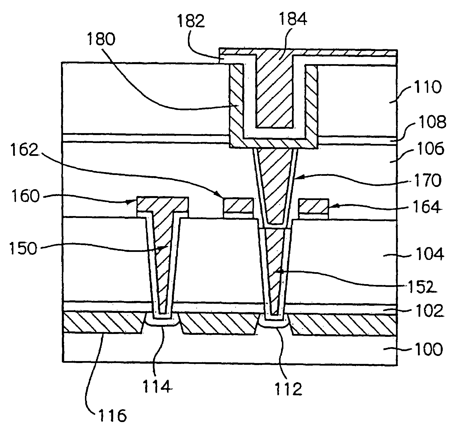
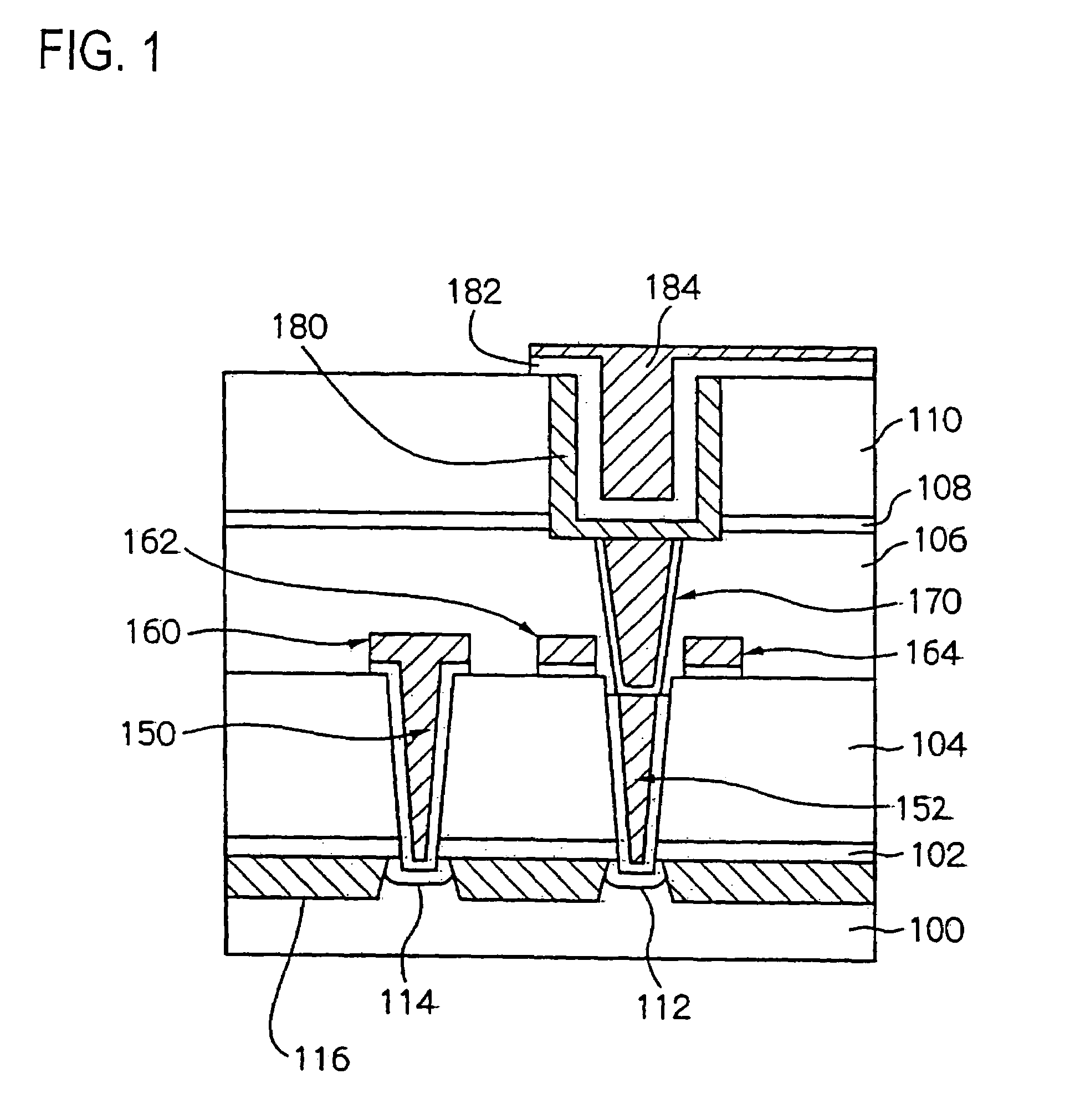
[0057]A constitution of a semiconductor device according to this working example will be described. The constitution described herein is based on a DRAM as in a conventional device.

[0058]FIG. 1 is a schematic cross-sectional view showing a constitution of a semiconductor device according to a first working example, which is a cross-sectional view of a memory cell region in a DRAM. In the subsequent passages, components referred to in the foregoing description are given an identical numeral, and detailed description thereof will be omitted.

[0059]As shown in FIG. 1, the semiconductor device is provided with a second cell contact plug 152 connected to a source electrode 112 of a transistor, and a capacitance contact plug 170 connected to the second cell contact plug 152.

[0060]In this working example, the silicon oxide layer 105 is not provided as an interlayer dielectric film unlike a conventional device. Accordingly, a distance between the second cell contact plug 152 and the lower el...

second working example

[0081]An advantageous feature of this working example is that an area of the cell contact plug that makes contact with the capacitance contact plug is recessed.

[0082]A constitution of a semiconductor device according to this working example is described hereunder.

[0083]FIG. 6 is a schematic cross-sectional view showing a constitution of a semiconductor device according to this working example. In the subsequent passages, components referred to in the first working example are given an identical numeral, and detailed description thereof will be omitted.

[0084]As shown in FIG. 6, a central region of a contact area of the second cell contact plug 158 with the capacitance contact plug 170 is recessed. Therefore, a contact area of the second cell contact plug 158 with the capacitance contact plug 170 becomes larger, and resultantly contact resistance is reduced.

[0085]Now a method of manufacturing of the semiconductor device according to this working example will be described. Here, detail...


PUM


Abstract

There is provided a method of manufacturing a semiconductor device that can reduce the number of processes, and decrease contact resistance between plugs. The method comprises forming a first interlayer dielectric film having a first opening where a contact plug is to be formed; uniformly forming a first conductive layer on the first interlayer dielectric film and in the first opening; forming a resist defining an interconnect pattern by a lithography process on a region excluding the first opening; performing first anisotropic etching to remove a region of the first conductive layer not covered with the resist until an upper face of the first interlayer dielectric film is exposed, thus to form an interconnect and the contact plug.

Description

[0001]This application is based on Japanese patent application No.2003-271016, the content of which is incorporated hereinto by reference.BACKGROUND OF THE INVENTION[0002]1. Field of the Invention[0003]The present invention relates to a semiconductor device and a method of manufacturing thereof.[0004]2. Description of the Related Art[0005]A constitution of a DRAM memory cell to be used in a semiconductor device, particularly a DRAM (Dynamic Random Access Memory) or a logic-embedded DRAM etc., as well as a method of manufacturing such memory cell have been disclosed in Japanese Patent laid open No.2003-007854.[0006]FIG. 8 is a schematic cross-sectional view showing a memory cell region formed in a conventional DRAM. Here, since transistors are similar to those disclosed in the cited document, detailed description thereof will be omitted.[0007]A DRAM memory cell is provided with a transistor formed on a semiconductor substrate 100 and a capacitance formed on the transistor via an inte...

Claims


Application Information

Patent Timeline
Patent Type & Authority Patents(United States)
IPC IPC(8): H01L21/4763H01L21/44H01L21/768H01L21/3213H01L21/8242H01L27/108
CPCH01L21/76804H01L21/76838H01L21/76877H01L27/10888H01L27/10855H01L27/10885H10B12/485H10B12/0335H10B12/482
Inventor SUGIMURA, HIROTOSHI
Owner RENESAS ELECTRONICS CORP
Why Eureka
Try Eureka