Check patentability & draft patents in minutes with Patsnap Eureka AI!

Light-emitting element

a technology of light-emitting elements and light-emitting elements, which is applied in the direction of basic electric elements, electrical apparatus, and semiconductor devices, can solve the problems of difficult to provide a sufficient luminance, and achieve the effect of higher luminan

Active Publication Date: 2012-07-19
ROHM CO LTD
View PDF0 Cites 19 Cited by
  • Summary
  • Abstract
  • Description
  • Claims
  • Application Information

AI Technical Summary

Benefits of technology

[0008]It is therefore a principal object of the present invention to provide a light-emitting element having a higher luminance.

Problems solved by technology

In the prior-art semiconductor light-emitting element, therefore, the light emitted from the light-emitting layer is extracted at a lower light extracting efficiency, making it difficult to provide a sufficient luminance.

Method used


Image

  • Light-emitting element
  • Light-emitting element
  • Light-emitting element

Examples


Embodiment Construction

[0057]An embodiment of the present invention will hereinafter be described in detail with reference to the attached drawings.

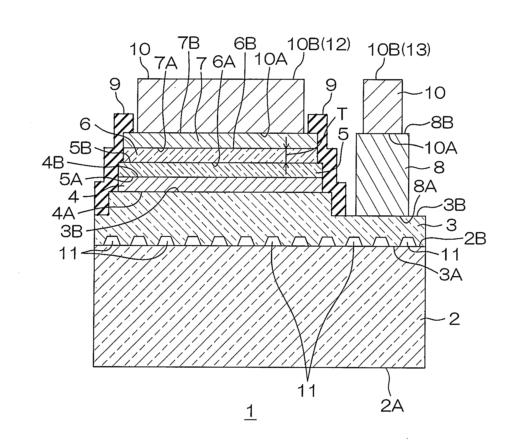
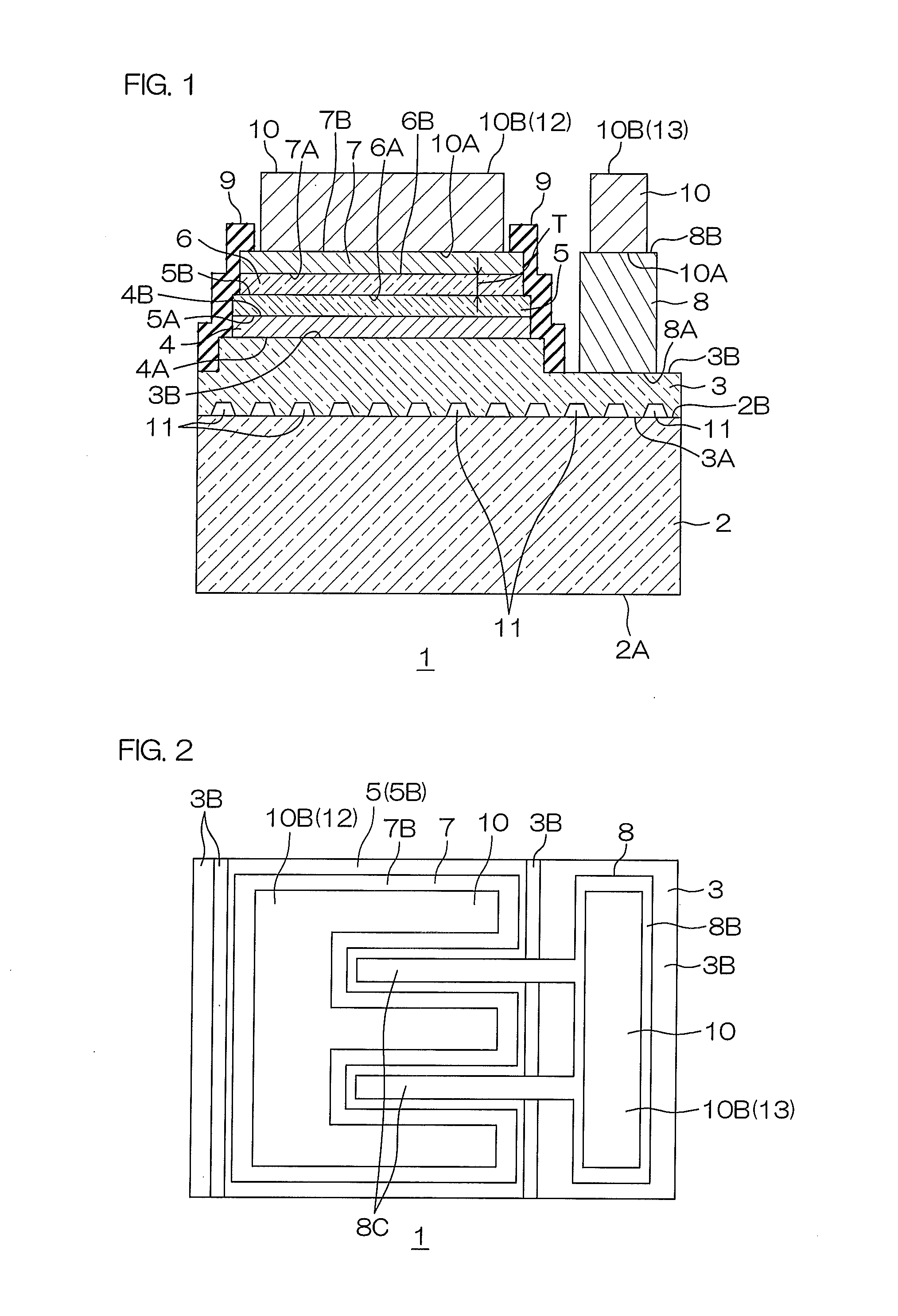
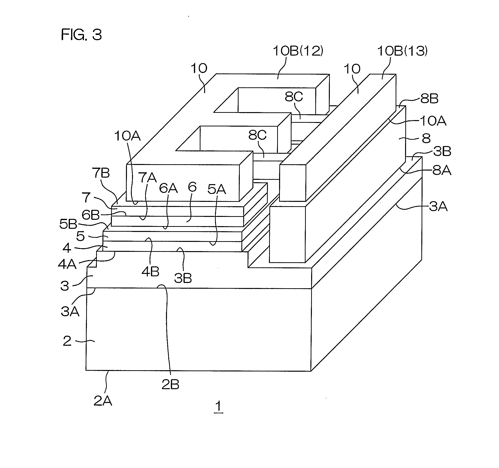
[0058]FIG. 1 is a schematic sectional view of a light-emitting element according to one embodiment of the present invention. FIG. 2 is a schematic plan view of the light-emitting element. FIG. 3 is a schematic perspective view of the light-emitting element.

[0059]The light-emitting element 1 includes a substrate 2, an n-type nitride semiconductor layer 3, a light-emitting layer 4, a p-type nitride semiconductor layer 5, a transparent electrode layer 6, a reflective electrode layer 7, an n-type electrode layer 8, an isolation insulative layer 9 and connection layers 10.

[0060]The n-type nitride semiconductor layer 3, the light-emitting layer 4, the p-type nitride semiconductor layer 5, the transparent electrode layer 6, the reflective electrode layer 7, the n-type electrode layer 8, the isolation insulative layer 9 and the connection layers 10 are provided on the...


PUM


Abstract

A light-emitting element, a light-emitting element unit and a light-emitting element package are provided, which are each reduced in reflection loss and intra-film light absorption by suppressing multiple light reflection in a transparent electrode layer and hence have higher luminance. The light-emitting element 1 includes a substrate 2, an n-type nitride semiconductor layer 3, a light-emitting layer 4, a p-type nitride semiconductor layer 5, a transparent electrode layer 6 and a reflective electrode layer 7, and the transparent electrode layer 6 has a thickness T satisfying the following expression (1):3λ4n+0.30×(λ4n)≤T≤3λ4n+0.45×(λ4n)(1)wherein λ is the light-emitting wavelength of the light-emitting element 4, and n is the refractive index of the transparent electrode layer 6.

Description

BACKGROUND OF THE INVENTION[0001]1. Field of the Invention[0002]The present invention relates to a light-emitting element, a light-emitting element unit including the light-emitting element, and a light-emitting element package including the light-emitting element unit and a resin package encapsulating the light-emitting element unit.[0003]2. Description of the Related Art[0004]One of prior-art semiconductor light-emitting elements is disclosed, for example, in JP-2008-263130A.[0005]A semiconductor light-emitting element disclosed in FIG. 4 of JP-2008-263130A includes a sapphire substrate through which light is extracted, a light-emitting layer, a transparent electrode and a reflective metal layer.[0006]When the light-emitting layer emits light, the light is mostly extracted through the sapphire substrate, but partly passes through the transparent electrode to be reflected on the reflective metal layer, and further passes through the transparent electrode to be extracted through the...

Claims


Application Information

Patent Timeline
IPC IPC(8): H01L33/42
CPCH01L33/38H01L33/42H01L33/405H01L33/005H01L33/385H01L33/387H01L2933/0016H01L2933/0025H01L2933/0066
Inventor FUJIMORI, TAKAONAKANISHI, YASUO
Owner ROHM CO LTD
Features
  • R&D
  • Intellectual Property
  • Life Sciences
  • Materials
  • Tech Scout
  • Unparalleled Data Quality
  • Higher Quality Content
  • 60% Fewer Hallucinations
Learn More