Method for Manufacturing a Structure, Optical Component, Optical Layer Stack

a manufacturing method and technology of optical microstructure, applied in the direction of optics, mountings, lenses, etc., can solve the problems of increasing the building length of optics, optical imaging errors, and stacking several lens wafers on top of each other with high precision, and achieves low deflection or bending, high lateral and axial precision of optical microstructure, and cost-effective

Active Publication Date: 2012-07-19
FRAUNHOFER GESELLSCHAFT ZUR FOERDERUNG DER ANGEWANDTEN FORSCHUNG EV
View PDF3 Cites 7 Cited by
  • Summary
  • Abstract
  • Description
  • Claims
  • Application Information

AI Technical Summary

Benefits of technology

[0013]It is thus one advantage of the present invention that by dissolving out the first structure cavities or air spaces may be created in an optical microstructure without stacking several glass substrates or polymer lens layers, as it is the case with the “monolithic lens technology”, which thus leads to a more cost-effective and also building height-reduced manufacturing with a high lateral and axial precision of the optical microstructure, as the otherwise existing request for mechanical stability of the individual layers which exist insulated from each other before joining is omitted.
[0014]Further, in some embodiments of the present invention, the substrate on which the structures were molded and cured may be removed, the same may thus be very thick and further mechanically stable and in particular comprise an extremely low deflection or bending.
[0015]According to one embodiment of the present invention, further a third structure of a third curable material may be formed and cured on a first surface of the second structure facing away from the substrate, so that at the first surface of the second structure a boundary surface between the second structure and the third structure is formed so that the second structure is not covered by the third structure at the passage area and the third curable material is insoluble for the solvent. The second curable material and the third curable material may comprise different refractive indices after curing.
[0016]It is thus a further advantage of the present invention, that lens stacks may be molded on top of each other by molding several structures of curable materials on top of each other without additional substrates with through holes which may only be manufactured and joined in high precision. Thus, with embodiments of the present invention, a costly stacking of the individual molded structures in high precision on top of each other is omitted. As compared to conventional technology, this leads to an increased cost reduction and to a setup with higher precision.
[0017]It is a further aspect of the present invention that an optical component of curable material comprises better optical characteristics when a cavity is adjacent to an optically relevant surface of curable material of the optical component.
[0018]It is thus an advantage of the present invention that an optical component comprises a boundary surface between an optically relevant surface which is for example a boundary surface for curable material and an air space. Embodiments may thus comprise a higher refractive index leap and thus a higher refractive power, due to a transition from a curable material to air, than it is the case with optical components with transitions from glass to glass or glass to curable material or other materials.

Problems solved by technology

On the one hand, the building length of the optics increases and on the other hand large lens thicknesses may lead to optical imaging errors.
Problems mainly result when stacking several lens wafers on top of each other with high precision.

Method used


Image

  • Method for Manufacturing a Structure, Optical Component, Optical Layer Stack
  • Method for Manufacturing a Structure, Optical Component, Optical Layer Stack
  • Method for Manufacturing a Structure, Optical Component, Optical Layer Stack

Examples


Embodiment Construction

[0043]Before the invention is explained in more detail in the following with reference to the drawings, it is noted that like elements in the figures are provided with the same or similar reference numerals and that a repeated description of these elements is omitted.

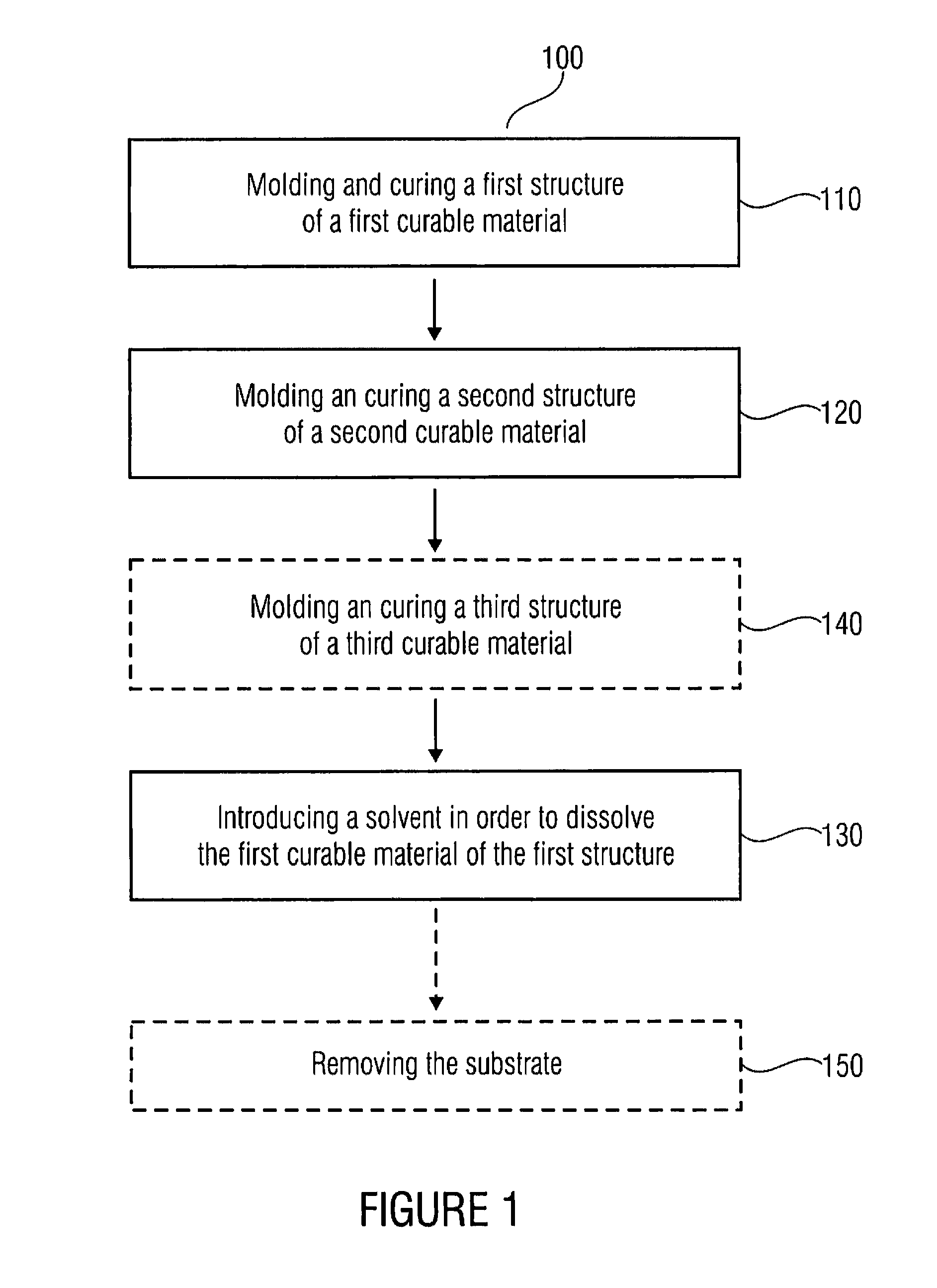
[0044]FIG. 1 shows a flowchart of a method 100 for manufacturing a structure of curable material according to one embodiment of the present invention.

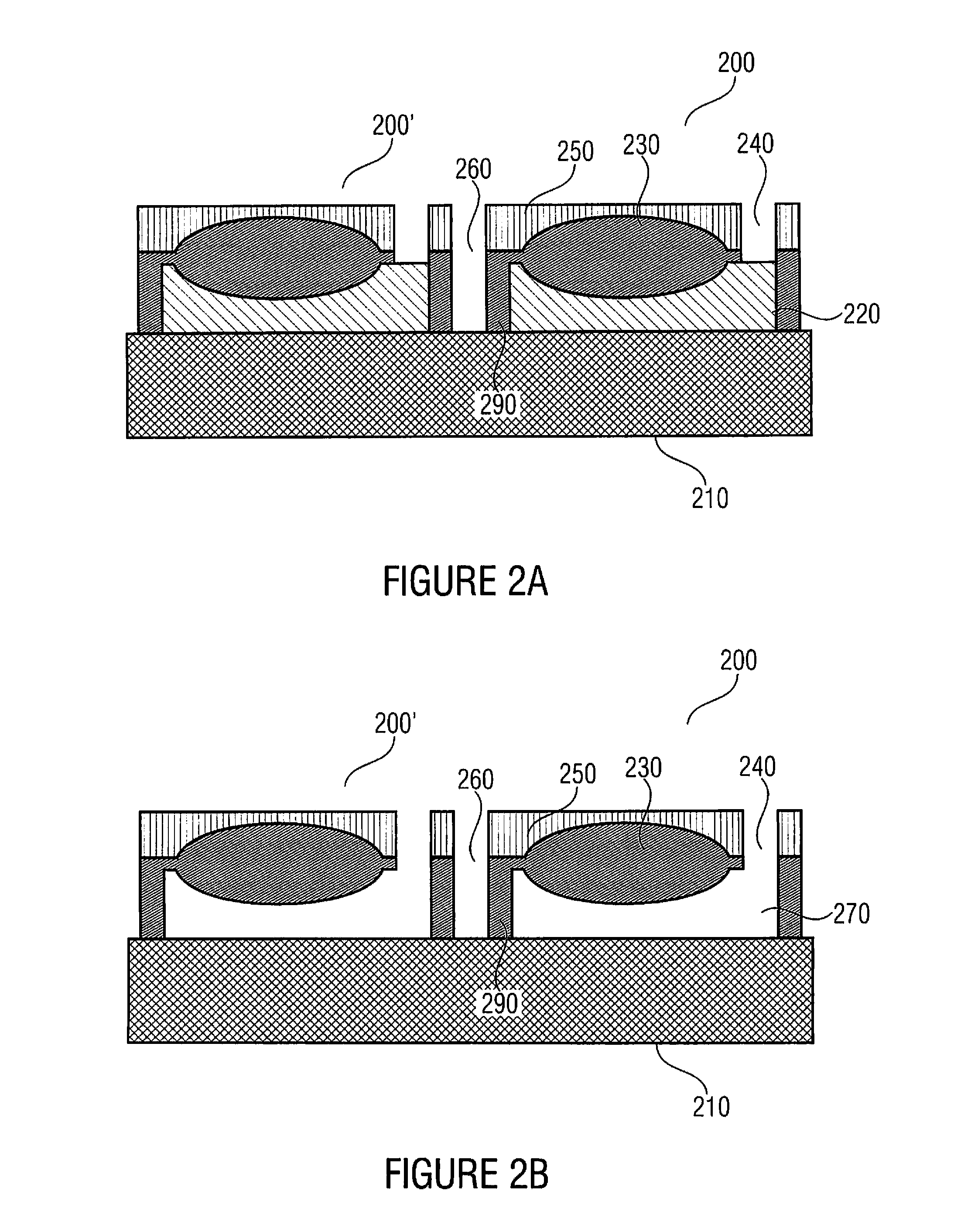
[0045]The method 100 includes a first step 110 of molding and curing a first structure of a first curable material on a substrate. Molding and curing may here be executed selectively regarding the location, so that a first area of a surface of the substrate is exposed.

[0046]Further, the method 100 includes a second step 120 of molding and curing a second structure of a second curable material on a first surface of the first structure facing away from the substrate so that at the first surface a boundary surface between the first structure and the second structure is formed...


PUM

PropertyMeasurementUnit
diameteraaaaaaaaaa
optical structureaaaaaaaaaa
wavelength rangeaaaaaaaaaa

Abstract

In a method for manufacturing a structure of curable material, a first structure from a first curable material is molded and cured on a substrate, and a second structure of a second curable material is molded and cured on a first surface of the first structure facing away from the substrate, so that at the first surface of the first structure a boundary surface forms between the first and second structures so that the first structure is not covered by the second structure in a passage area. A solvent is introduced into the passage area to dissolve the first curable material of the first structure so that a cavity forms between the second structure and the first surface of the substrate. After curing, the first curable material is soluble and the second curable material is insoluble for the solvent. An optical component and an optical layer stack are made of curable material.

Description

CROSS-REFERENCE TO RELATED APPLICATIONS[0001]This application is a continuation of copending International Application No. PCT / EP2010 / 069293, filed Dec. 9, 2010, which is incorporated herein by reference in its entirety, and additionally claims priority from German Application No. 102009055088.7-51, filed Dec. 21, 2009, which is also incorporated herein by reference in its entirety.[0002]The present invention relates to a concept for manufacturing a structure of curable material, like for example an optical lens.BACKGROUND OF THE INVENTION[0003]The parallelized manufacturing of optical microstructures in panels, like e.g. lenses for micro objectives for being used in mobile telephones, is based on the use of glass substrates onto which the optical structures are applied, e.g. by UV replication. FIG. 10a shows a lens reproduced or molded on a glass substrate by UV replication.[0004]For mechanical reasons the substrates may fall below a critical thickness neither during manufacturing ...

Claims


Application Information

Patent Timeline
Patent Type & Authority Applications(United States)
IPC IPC(8): G02B3/00B29D11/00
CPCB29C33/52B29D11/00009G02B3/00G02B13/0085B29L2011/00B29D11/00
Inventor WIPPERMANN, FRANKDUPARRÉ, JACQUESDANNBERG, PETERBRAEUER, ANDREAS
Owner FRAUNHOFER GESELLSCHAFT ZUR FOERDERUNG DER ANGEWANDTEN FORSCHUNG EV
Why Eureka
Try Eureka