Waveguide conversion device

a conversion device and waveguide technology, applied in the field of electronic communication technologies, can solve the problems of poor performance consistency and complex assembly, and achieve the effect of improving electrical performance consistency and reducing assembly difficulty

Inactive Publication Date: 2012-07-26
HUAWEI TECH CO LTD
View PDF6 Cites 15 Cited by
  • Summary
  • Abstract
  • Description
  • Claims
  • Application Information

AI Technical Summary

Benefits of technology

[0013]In the embodiments of the present application, a waveguide conversion device is disposed on a multi-layer circuit board, so that the waveguide conversion device and a transceiver system can be conveniently integrated on a multi-layer circuit board, thereby improving the electrical performance consistency between the waveguide conversion device and the transceiver system or other components on the multi-layer circuit board and reducing assembly difficulty.

Problems solved by technology

Therefore, when the two-layer board is assembled to the multi-layer board, the requirement for accuracy of positioning is high, the assembly is complex, and performance consistency is poor.

Method used


Image

  • Waveguide conversion device
  • Waveguide conversion device
  • Waveguide conversion device

Examples


Embodiment Construction

[0021]The technical solutions of the present application will be clearly and completely described in the following with reference to the accompanying drawings. It is obvious that the embodiments to be described are only a part rather than all of the embodiments of the present application. All other embodiments obtained by persons of ordinary skill in the art based on the embodiments of the present application without creative efforts shall fall within the protection scope of the present application.

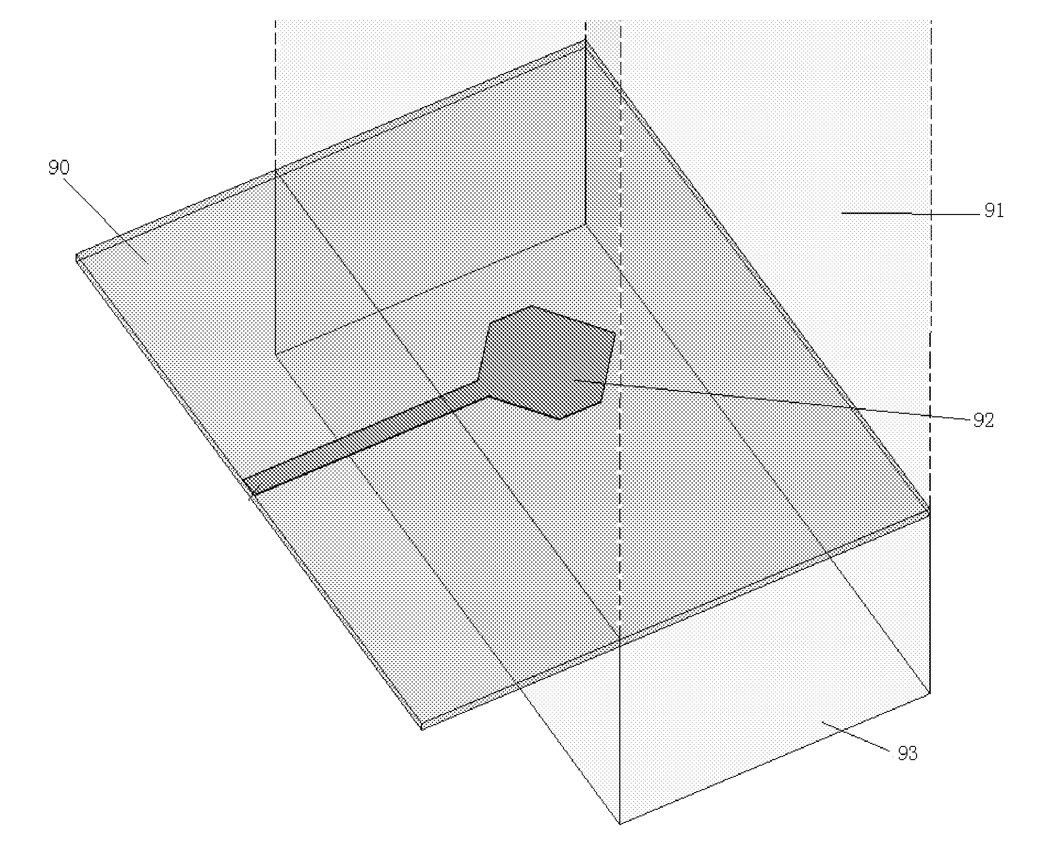
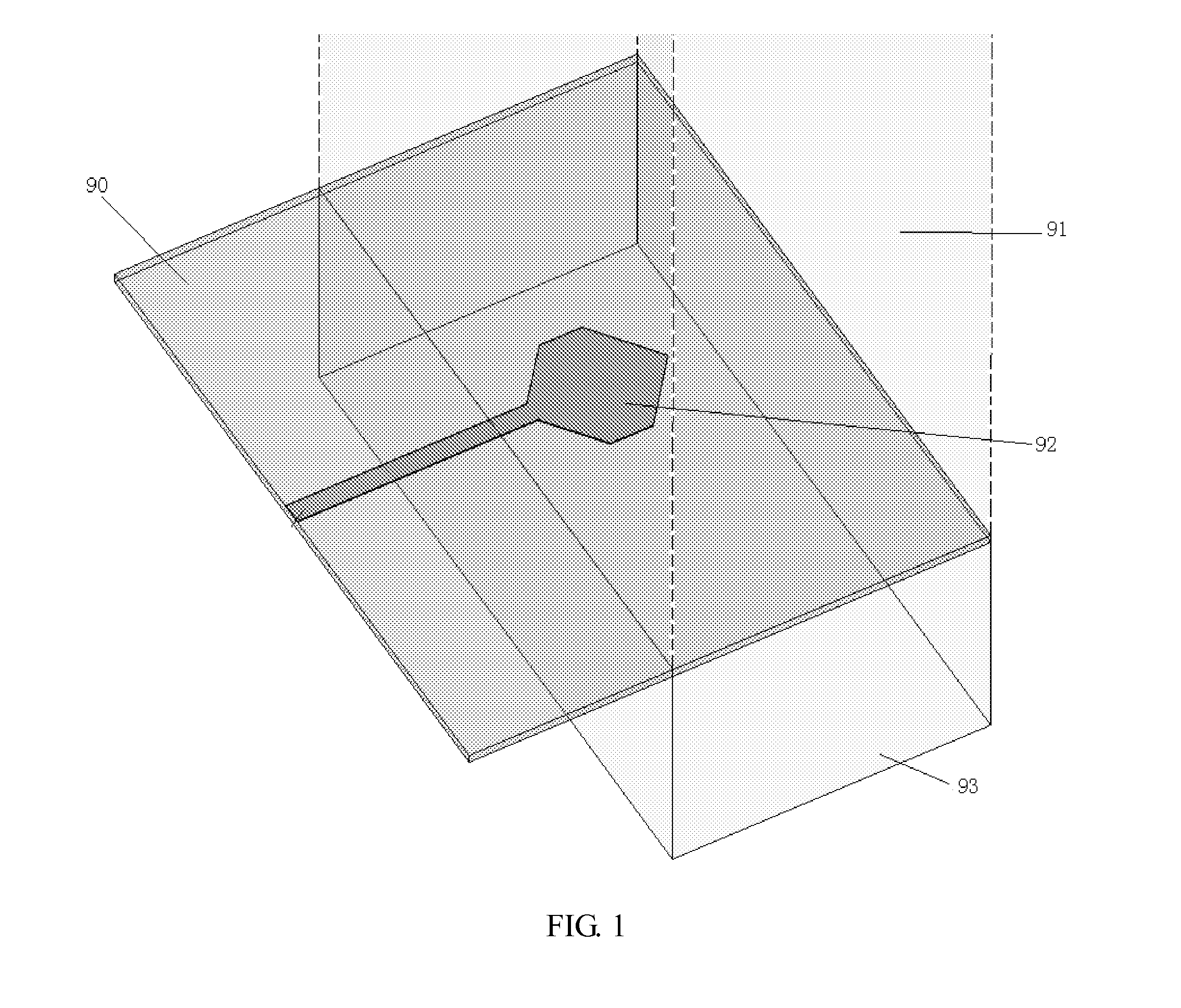
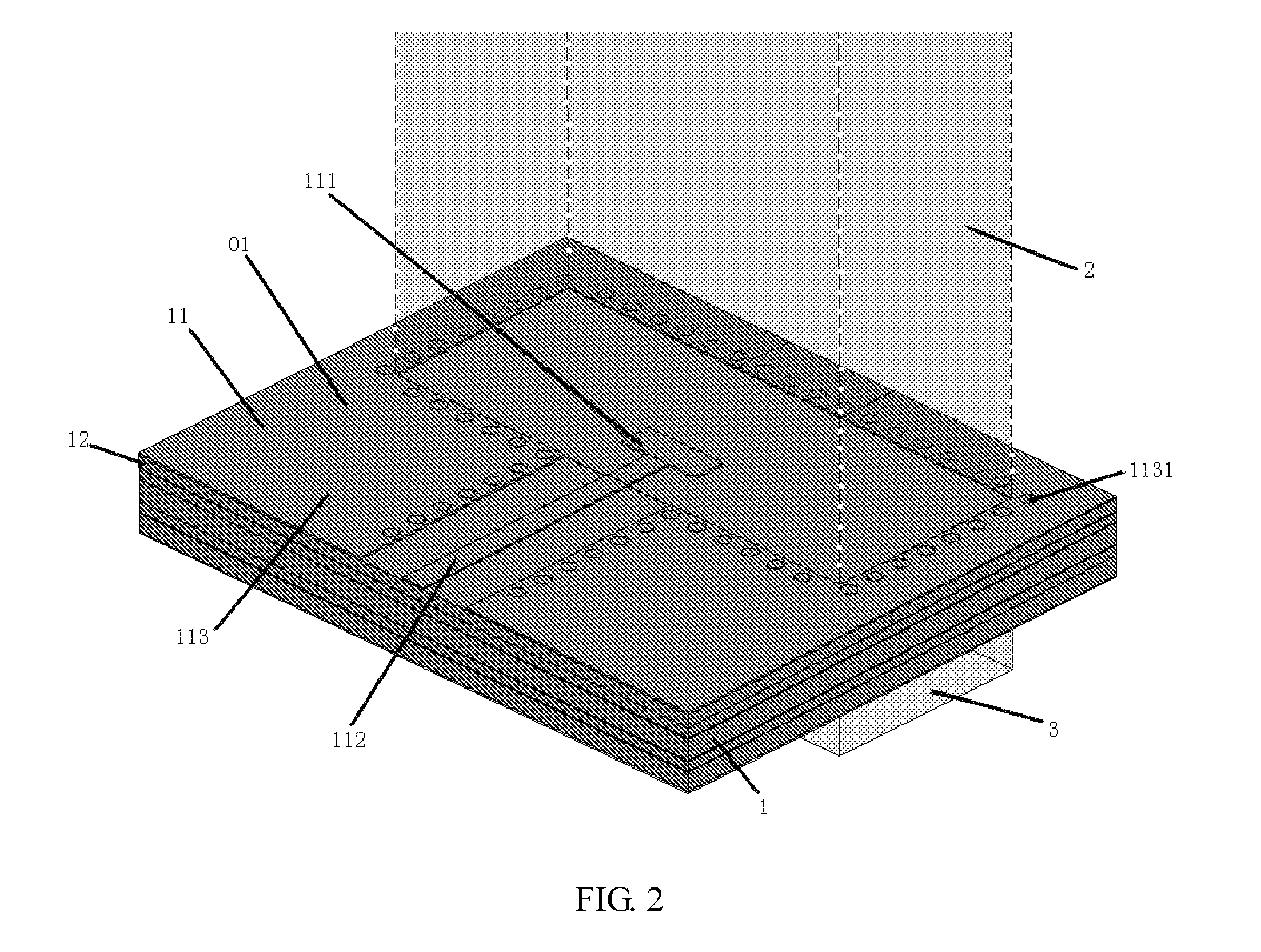
[0022]As shown in FIG. 2, an embodiment of the present application provides a waveguide conversion device, where the waveguide conversion device includes: a multi-layer circuit board 1; and a waveguide cavity 2 and a metal reflection cavity 3 located at two lateral sides of the multi-layer circuit board 1. The metal reflection cavity 3 and the waveguide cavity 2 are embedded in the multi-layer circuit board 1. The multi-layer circuit board 1 is disposed with a micro strip line or a strip ...


PUM


Abstract

Embodiments of the present application disclose a waveguide conversion device. The waveguide conversion device includes: a multi-layer circuit board; and a waveguide cavity and a metal reflection cavity, located at two lateral sides of the multi-layer circuit board. The waveguide cavity and the metal reflection cavity are embedded in the multi-layer circuit board. The multi-layer circuit board is disposed with a micro strip line or a strip line and a match patch connected to the micro strip line or the strip line. The match patch is located in the waveguide cavity.

Description

CROSS-REFERENCE TO RELATED APPLICATIONS[0001]This application is a continuation of International Application No. PCT / CN2010 / 079264, filed on Nov. 30, 2010, which claims priority to Chinese Patent Application No. 200910188486.5, filed on Nov. 30, 2009, both of which are hereby incorporated by reference in their entireties.FIELD OF THE APPLICATION[0002]The present application relates to the field of electronic communications technologies, and in particular, to a waveguide conversion device.BACKGROUND OF THE APPLICATION[0003]A waveguide conversion device is used in a microwave transceiver system, as shown in FIG. 1. an existing waveguide conversion device is disposed on a two-layer circuit board 90, and the two-layer circuit board is disposed with a micro strip line match patch 92, and a waveguide cavity 91 and a metal reflection cavity 93 are disposed at two lateral sides of the two-layer circuit board 90.[0004]To achieve communication connection with a transceiver system located at a...

Claims


Application Information

Patent Timeline
Patent Type & Authority Applications(United States)
IPC IPC(8): H01P3/08
CPCH01P5/107
Inventor LIU, JIEGUO, CUIYUAN, WENXINYU, TIEZHU
Owner HUAWEI TECH CO LTD
Why Eureka
Try Eureka