RFID transponder and method for connecting a semiconductor die to an antenna

a technology of rfid transponder and semiconductor die, which is applied in the direction of instruments, soldering devices, manufacturing tools, etc., can solve the problems of more than 70% of cost saving, and achieve the effect of reducing mechanical stress for the antenna to die connection

Inactive Publication Date: 2012-08-02
TEXAS INSTR INC
View PDF6 Cites 64 Cited by
  • Summary
  • Abstract
  • Description
  • Claims
  • Application Information

AI Technical Summary

Benefits of technology

[0004]It is a general object of the invention to provide an RFID transponder comprising a semiconductor die and an antenna made from a winding wire and a method for connecting a semiconductor die to the winding wire of an antenna offering reduced mechanical stress for the antenna to die connection.

Problems solved by technology

The expensive gold layer in the contact area may be omitted which leads to more than 70% of cost saving.

Method used


Image

  • RFID transponder and method for connecting a semiconductor die to an antenna
  • RFID transponder and method for connecting a semiconductor die to an antenna

Examples


Embodiment Construction

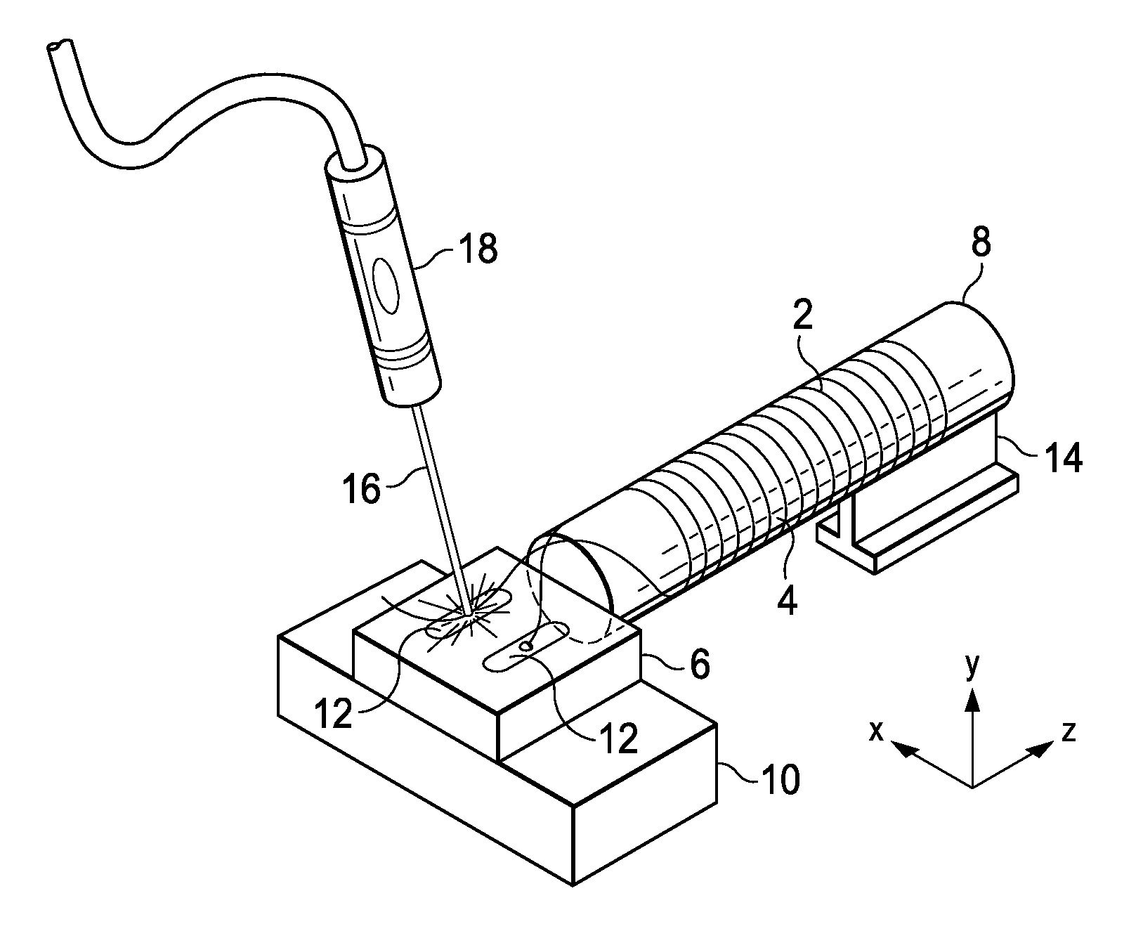
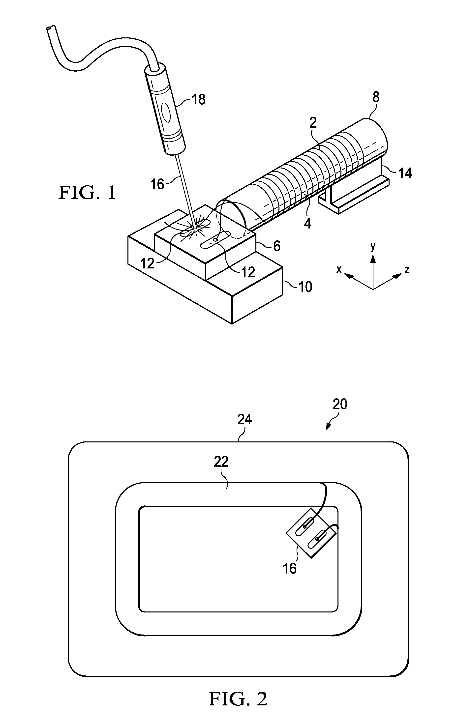
[0020]FIG. 1 is a simplified perspective view showing a system for connecting the winding wire 2 of an antenna 4 to a die 6. The winding wire 2 of the antenna 4 is located on a suitable core 8, preferably a ferrite core. The principles of connecting the antenna's winding wire 2 to the die 6 are not limited to an antenna 4 having the depicted structure. Other winding wires 2 may be connected to the die 6 in the same way.

[0021]The semiconductor die 6 is located on a positioning stage 10 for positioning the die 6 relative to the antenna 4 and a connecting end of the winding wire 2. The die 6 comprises solderable contact areas 12, preferably a metal plating made from a nickel based alloy, e.g., a NiAu or a NiSn alloy. The solderable contact areas are positioned underneath the soldering end of the winding wire 2 of the antenna 4 with the help of the positioning stage 6. This is preferably done automatically. A suitable solder material, preferably a lead and flux free solder alloy, may be...


PUM

PropertyMeasurementUnit
temperaturesaaaaaaaaaa
areaaaaaaaaaaa
thermalaaaaaaaaaa

Abstract

An RFID transponder having a semiconductor die with a solderable contact area and an antenna made from a winding wire, wherein the winding wire is soldered to the contact area, and the solderable contact area is made from a nickel based alloy.

Description

CROSS-REFERENCE TO RELATED APPLICATIONS[0001]This patent application claims priority from German Patent Application No. 10 2011 009 577.2, filed Jan. 27, 2011, which is incorporated herein by reference in its entirety.FIELD OF THE INVENTION[0002]The invention relates to an RFID transponder, comprising a semiconductor die and an antenna made from a winding wire. Further, the invention relates to a method for connecting a semiconductor die to an antenna winding wire.BACKGROUND OF THE INVENTION[0003]Current wafers for transponder chips, especially for RFID HDX transponders, need expensive gold layers for contacting the same to a winding wire of an antenna. Further, the antenna's winding wire needs to be soldered manually which causes a long process time and additional costs. Soldering is typically performed by a thermo compression process that is known to create high thermal and mechanical stress to the respective material in the soldering area. Intrinsic stress may lead to degradation...

Claims


Application Information

Patent Timeline
Patent Type & Authority Applications(United States)
IPC IPC(8): H01L23/49H01P11/00B23K26/00B23K31/02B23K1/20
CPCG06K19/07754Y10T29/49016H01L2224/4813
Inventor GROSS, JOHANNLANGE, BERNHARD
Owner TEXAS INSTR INC
Why Eureka
Try Eureka