Memory circuit

Inactive Publication Date: 2012-08-02
SEMICON ENERGY LAB CO LTD
View PDF4 Cites 26 Cited by
  • Summary
  • Abstract
  • Description
  • Claims
  • Application Information

AI Technical Summary

Benefits of technology

[0019]In the memory circuit of a signal processing unit according to one embodiment of the present invention, the booster circuit may include a booster transistor whose gate is electrically connected to whose one of a source and a drain, and may boost a potential by a bootstrapping method in which the gate of the first transistor is brought into an electrically floating state by the bo

Problems solved by technology

The method in which a data signal that has been held in a volatile memory circuit is held in a nonvolatile memory circuit located in the periphery of the volatile memory circuit while a supply of power to a signal processing unit is stopped involves a complicated process of manufacturing the signal processing unit because a magnetic element or a ferroelectric is used in the nonvolatile memory circuit in many cases.
With the method in which a data signal that

Method used


Image

  • Memory circuit
  • Memory circuit
  • Memory circuit

Examples


embodiment 1

[0057]A signal processing unit includes a memory circuit. The memory circuit can store a data signal of one-bit or multi-bit by one or more memory circuits provided. This embodiment describes a configuration of the memory circuit in the signal processing unit.

[0058]Note that examples of the signal processing unit according to the preset invention include, in its category, large scale integrated circuits (LSIs) such as CPUs, microprocessors, image processing circuits, digital signal processors (DSPs), and field programmable gate arrays (FPGAs).

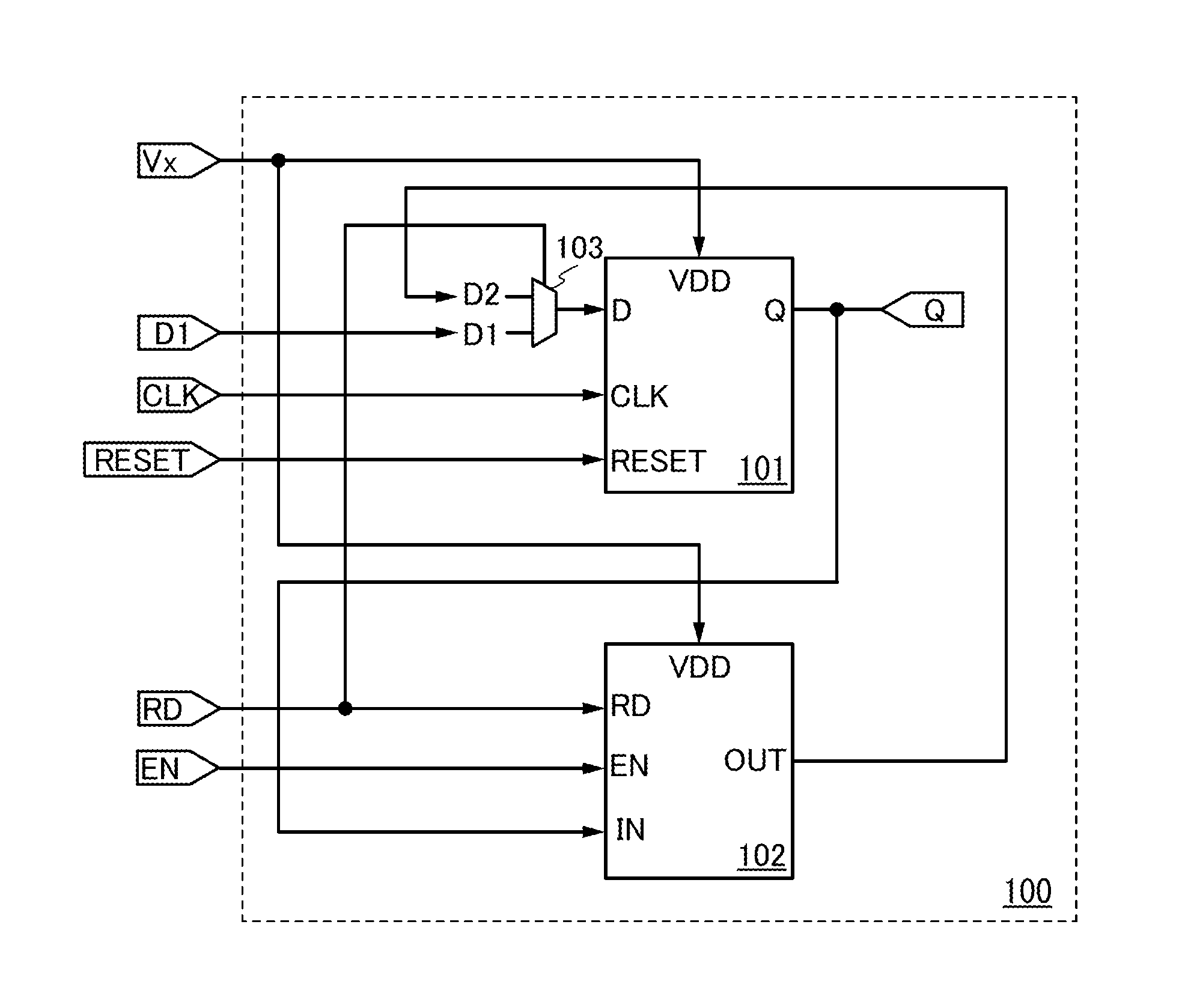
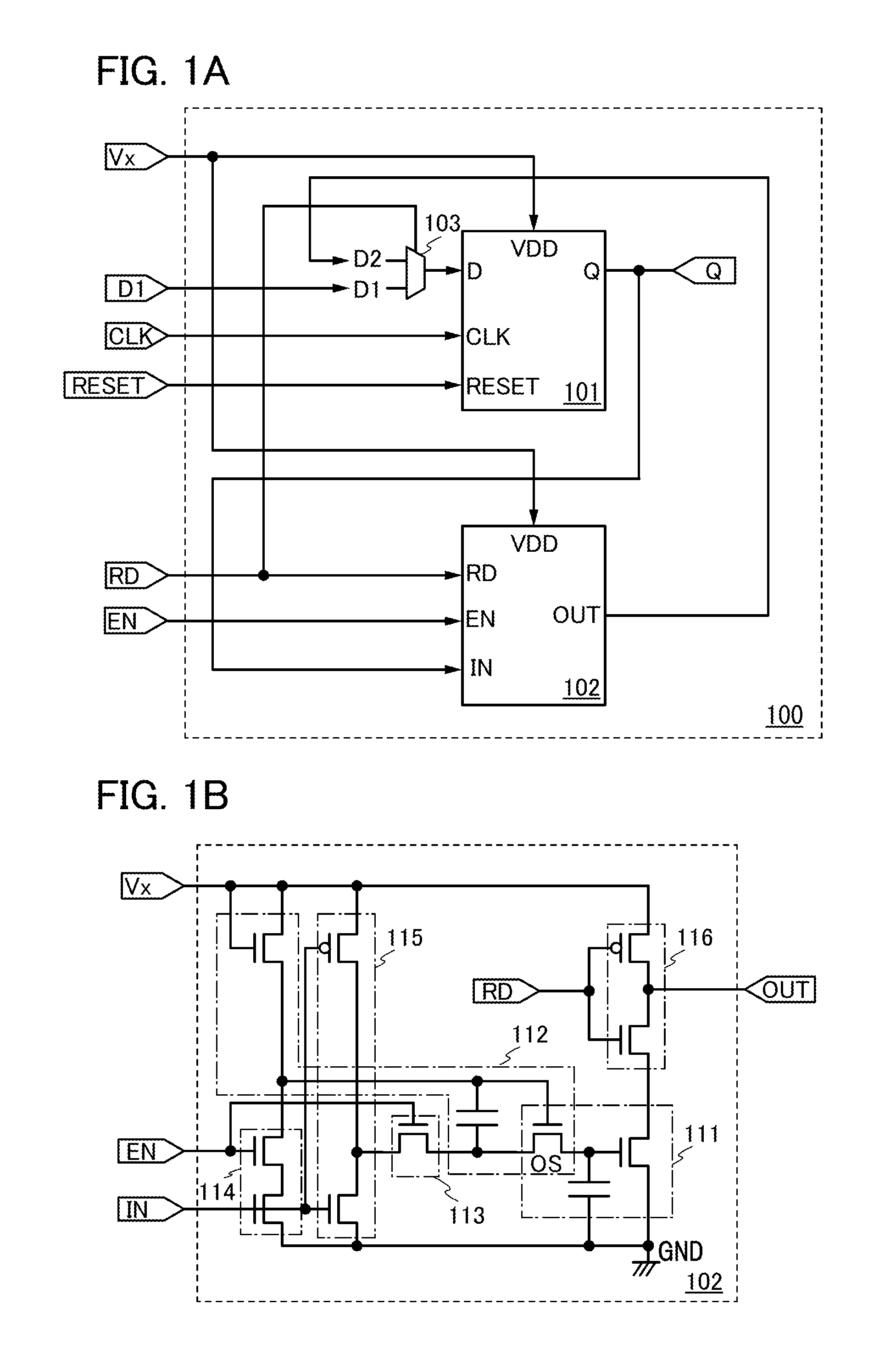
[0059]FIG. 1A shows an example of a block diagram of the memory circuit. A memory circuit 100 shown in FIG. 1A roughly includes a volatile memory section 101 and a nonvolatile memory section 102 and includes a selector circuit 103 at an input terminal side of the volatile memory section 101.

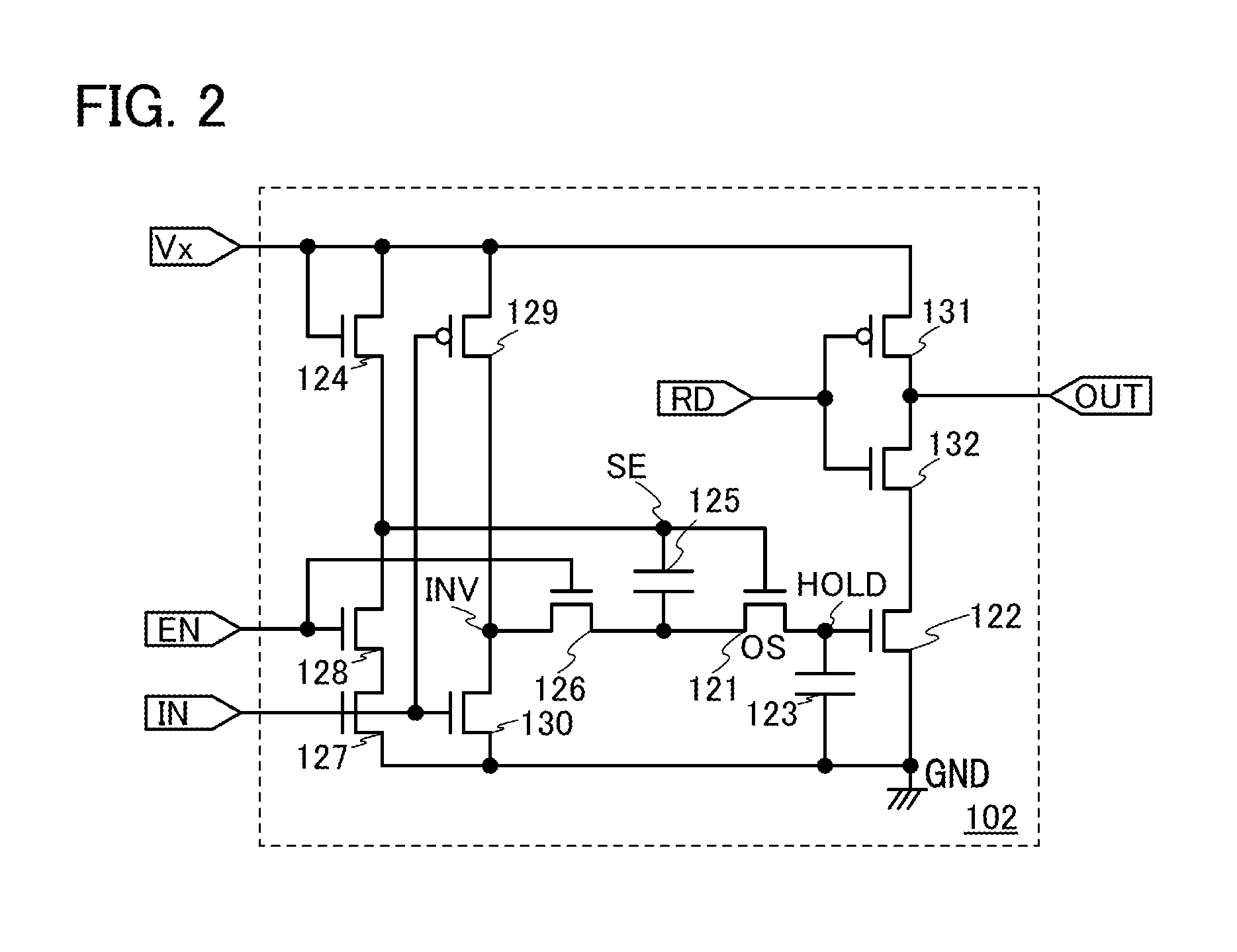
[0060]The volatile memory section 101 includes, for example, a reset flip-flop circuit which is a clock synchronization type. Note that the flip-flop circui...

embodiment 2

[0126]This embodiment describes a structure including a plurality of memory circuits each shown in Embodiment 1.

[0127]FIG. 9A shows an example of the structure of a memory circuit according to Embodiment 2. The memory circuit shown in FIG. 9A includes a phase inverter circuit 401 to which the high power supply potential VDD and the low power supply potential VSS are supplied, and a memory circuit group 403 including a plurality of memory circuits 402. Specifically, the memory circuit 100 according to Embodiment 1 can be used as each memory circuit 402. The high power supply potential VDD or the low power supply potential VSS is applied via the phase inverter circuit 401 to each memory circuit 402 included in the memory circuit group 403. In addition, the potential of the signal IN and the low power supply potential VSS are applied to each memory circuit 402 included in the memory circuit group 403.

[0128]In FIG. 9A, output of the phase inverter circuit 401 is switched between the hig...

embodiment 3

[0131]This embodiment describes a structure of a signal processing unit including a memory circuit described in Embodiment 1 or a memory circuit described in Embodiment 2.

[0132]FIG. 10 illustrates an example of a signal processing unit according to an embodiment of the present invention. The signal processing unit includes at least one or more arithmetic units and one or more memory circuits. Specifically, a signal processing unit 150 illustrated in FIG. 10 includes an arithmetic unit 151, an arithmetic unit 152, a memory circuit 153, a memory circuit 154, a memory circuit 155, a control unit 156, and a power control circuit 157.

[0133]The arithmetic units 151 and 152 each include, as well as a logic circuit which carries out simple logic arithmetic processing, an adder, a multiplier, and various arithmetic units. The memory circuit 153 functions as a register for temporarily holding a data signal when the arithmetic processing is carried out in the arithmetic unit 151. The memory ci...


PUM


Abstract

The present invention provides a memory circuit in which, while the power is not supplied, a data signal that has been held in a memory section corresponding to a volatile memory can be held in a capacitor in a memory section corresponding to a nonvolatile memory. In the nonvolatile memory section, a transistor whose channel is formed in an oxide semiconductor layer allows a signal to be held in the capacitor for a long period. Thus, the memory circuit can hold a logic state (data signal) even while the power supply is stopped. A potential applied to a gate of the transistor whose channel is formed in an oxide semiconductor layer is raised by a booster circuit provided between a wiring for carrying power supply potential and the gate of the transistor, allowing a data signal to be held even by one power supply potential without malfunction.

Description

BACKGROUND OF THE INVENTION[0001]1. Field of the Invention[0002]The present invention relates to a memory circuit in a signal processing unit, in which the logic state is not erased after the power is turned off.[0003]2. Description of the Related Art[0004]Signal processing units such as central processing units (CPUs) vary in structure depending on the intended use. A signal processing unit generally has a main memory for storing data or program and other memory circuits such as a register and a cache memory. A register has a function of temporarily holding a data signal for carrying out arithmetic processing, holding a program execution state, or the like. Meanwhile, a cache memory, which is located between an arithmetic unit and a main memory, is provided to reduce low-speed access to the main memory and speed up the arithmetic processing.[0005]In a memory circuit in a signal processing unit, such as a register or a cache memory, input of a data signal needs to be performed at hi...

Claims


Application Information

Patent Timeline
IPC IPC(8): G11C14/00
CPCG11C14/0063H01L21/8258H01L27/0688H01L27/1156H01L27/1207G11C14/0018G11C11/34G11C11/41G11C14/00H01L29/788H01L29/792G11C5/14H01L27/1225H10B41/70
Inventor OHMARU, TAKURO
Owner SEMICON ENERGY LAB CO LTD
Why Eureka
Try Eureka