

Microwave irradiation apparatus
- Summary
- Abstract
- Description
- Claims
- Application Information
AI Technical Summary
Benefits of technology
Problems solved by technology
Method used
Image

Examples
Embodiment Construction
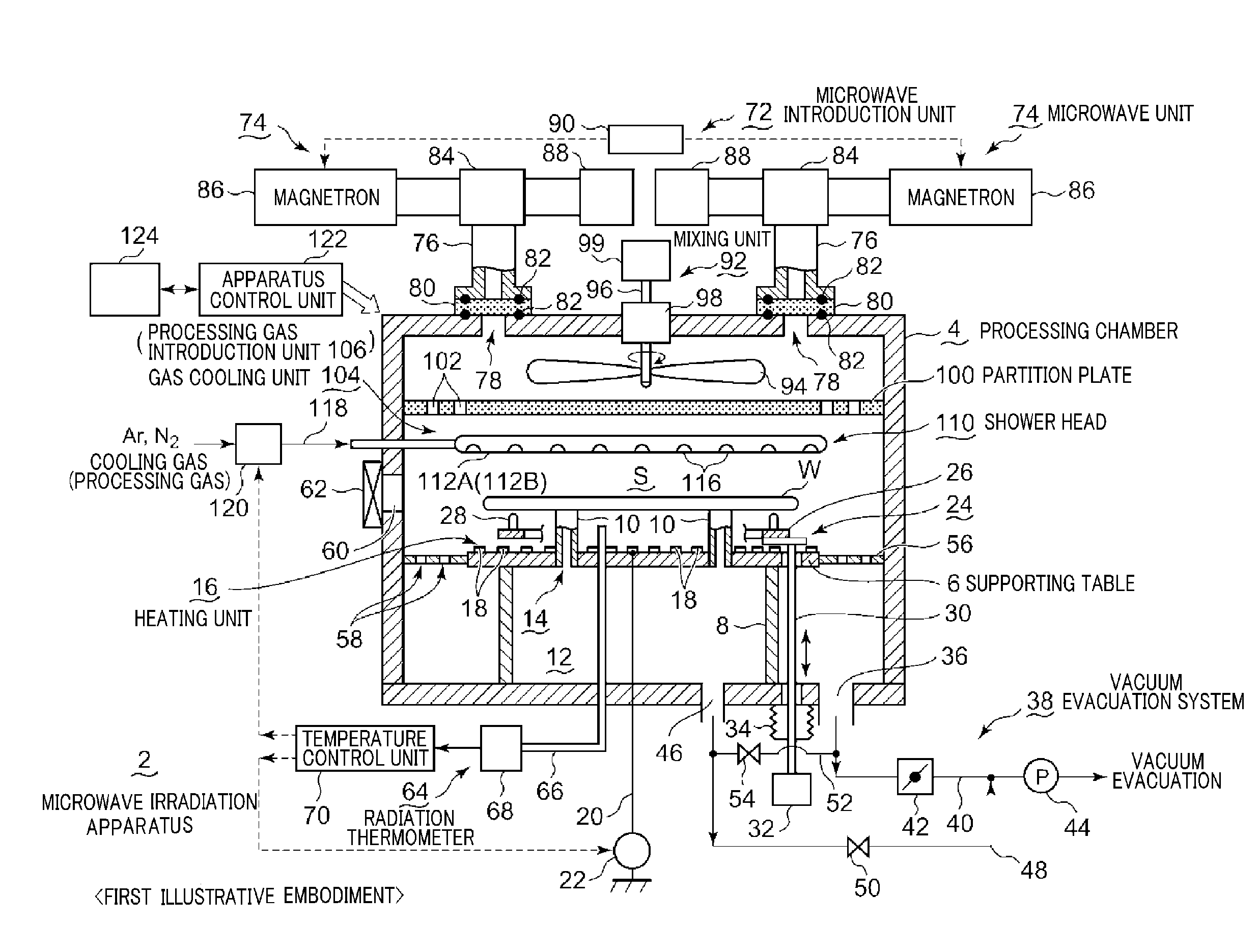
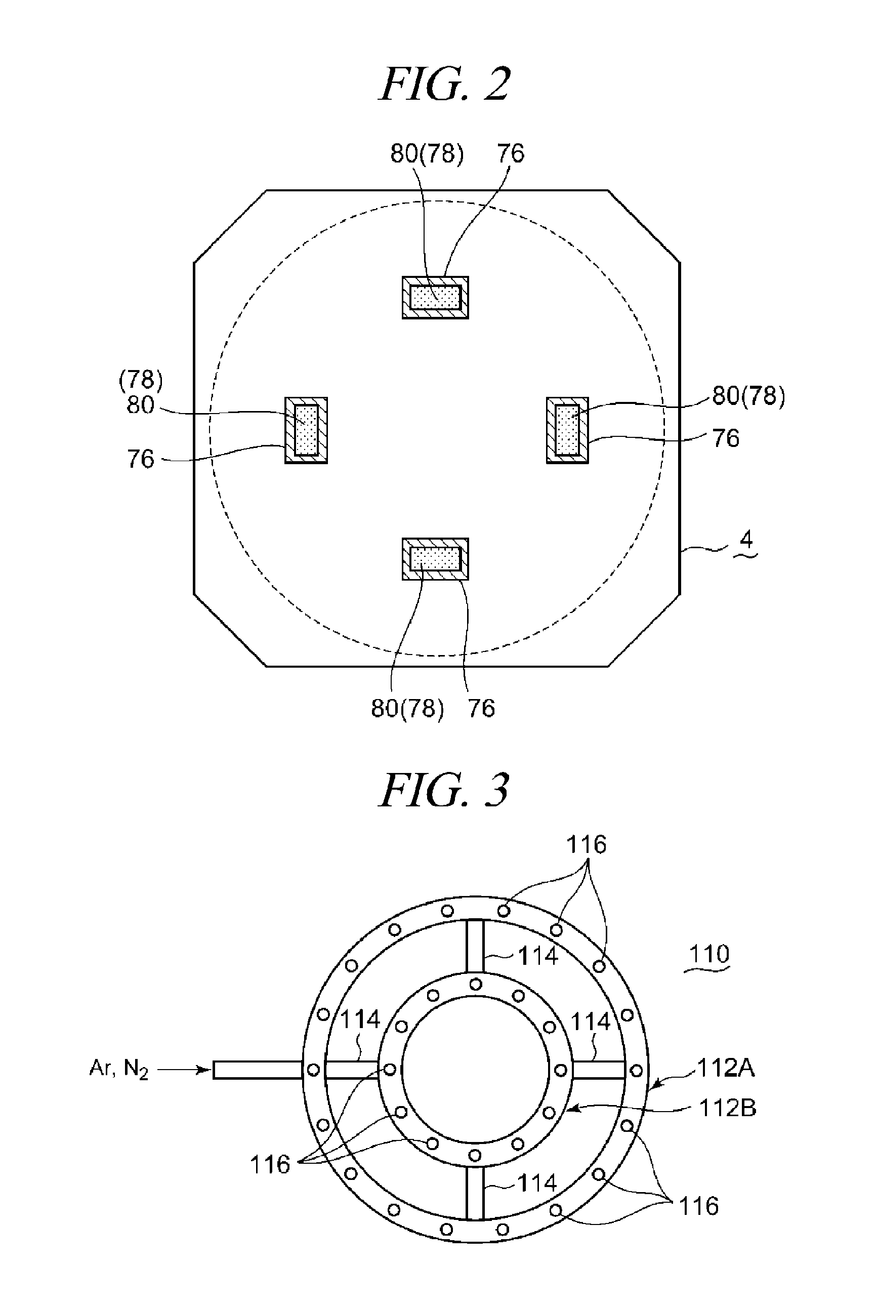
[0029]Hereinafter, a microwave irradiation apparatus in accordance with an illustrative embodiment will be described with reference to the accompanying drawings. FIG. 1 is a configuration view showing a microwave irradiation apparatus in accordance with a first illustrative embodiment. FIG. 2 shows waveguides of a microwave introduction unit positioned at a ceiling of a processing chamber. FIG. 3 shows a bottom surface of a shower head of a gas cooling unit (a processing gas introduction unit).
First Illustrative Embodiment
[0030]As depicted in the drawings, a microwave irradiation apparatus 2 includes a cylindrical processing chamber 4 made of aluminum, an aluminum alloy or stainless steel, and the inside of processing chamber 4 has a circular cross section shape. Within the processing chamber 4, a supporting table having a circular plate shape is supported by a cylindrical supporting column 8 standing uprightly from a bottom portion of the processing chamber 4. The supporting table ...
PUM
 Abstract
Description
Claims
Application Information