Solid-state imaging element and imaging device

a solid-state imaging and imaging element technology, applied in the field of solid-state imaging elements and imaging devices, can solve the problems of reducing the optical efficiency of the camera, the decrease of the optical efficiency of the color filter, and the low intensity of the light falling on a single pixel, so as to achieve a optical efficiency. , the effect of high degree of color reproducibility

Inactive Publication Date: 2012-08-23
SOVEREIGN PEAK VENTURES LLC
View PDF6 Cites 43 Cited by
  • Summary
  • Abstract
  • Description
  • Claims
  • Application Information

AI Technical Summary

Benefits of technology

[0033]In a solid-state image sensor according to the present invention, a dispersing element that disperses incoming light according to the wavelength range is arranged on its imaging area, and a color filter that either absorbs or reflects a light ray falling within some wavelength range is arranged between the pixels and the dispersing element. If the color filter is designed so as to have an ideal dispersing property according to the property of the dispersing element, the photoelectrically converted signal to be supplied from a pixel that receives the light that has been transmitted through that color filter can be even closer to an ideal one. In other words, even if the dispersing property of the dispersing element is slightly different from the designed one, a signal variation to be caused due to that slight difference can be compensated for by the color filter. Consequently, the image sensor of the present invention can capture an image with a higher degree of color reproducibility than a situation where a conventional image sensor is used. According to the present invention, even though the incoming light is partially lost by the color filter, that loss results from the slight difference of the dispersing property of the dispersing element from the designed one, and therefore, is very little. That is why the present invention provides an image capture device that achieves a high degree of color reproducibility and optical efficiency.

Problems solved by technology

Nevertheless, the greater the number of pixels in an image sensor, the lower the intensity of the light falling on a single pixel and the lower the sensitivity of camera tends to be.
That is why with such a color filter, the optical efficiency of a camera would decrease.
It is true that the aperture ratio can be increased substantially by this technique but the decrease in optical efficiency by color filters still persists.
As a result, only a required component of the incoming light falling within a particular wavelength range can be incident on each photosensing section with causing a significant loss of the incoming light.
That is why to detect light rays in the three primary colors of RGB, for example, the number of photosensitive cells provided should be tripled compared to a situation where conventional color filters are used, which is a problem.
Nevertheless, even if such a technique is adopted, the optical efficiency cannot be 100% since one out of the three colors should be sacrificed.

Method used


Image

  • Solid-state imaging element and imaging device
  • Solid-state imaging element and imaging device
  • Solid-state imaging element and imaging device

Examples


embodiment 1

[0082]FIG. 6 is a block diagram illustrating an overall configuration for an image capture device as a first preferred embodiment of the present invention. The image capture device of this preferred embodiment is a digital electronic camera and includes an image capturing section 500 and a signal processing section 400 that receives a signal from the image capturing section 500 and outputs a signal representing an image (i.e., an image signal). The image capture device may either generate only a still picture or have the function of generating a moving picture.

[0083]The image capturing section 500 includes an optical lens 12 for imaging a given subject, an optical filter 11, a solid-state image sensor 10 (which will be simply referred to herein as an “image sensor”) for converting the optical information that has been gotten through the optical lens 12 and the optical filter 11 into an electrical signal by photoelectric conversion. The image capturing section 500 further includes a ...

embodiment 2

[0124]Next, a second specific preferred embodiment of the present invention will be described with reference to FIGS. 11A through 11C. The image capture device of this preferred embodiment has the same configuration as the counterpart of the first preferred embodiment described above except the structure of the image sensor 10. Thus, the following description of this second preferred embodiment will be focused on only the difference from the first preferred embodiment and description of their common features will be omitted herein.

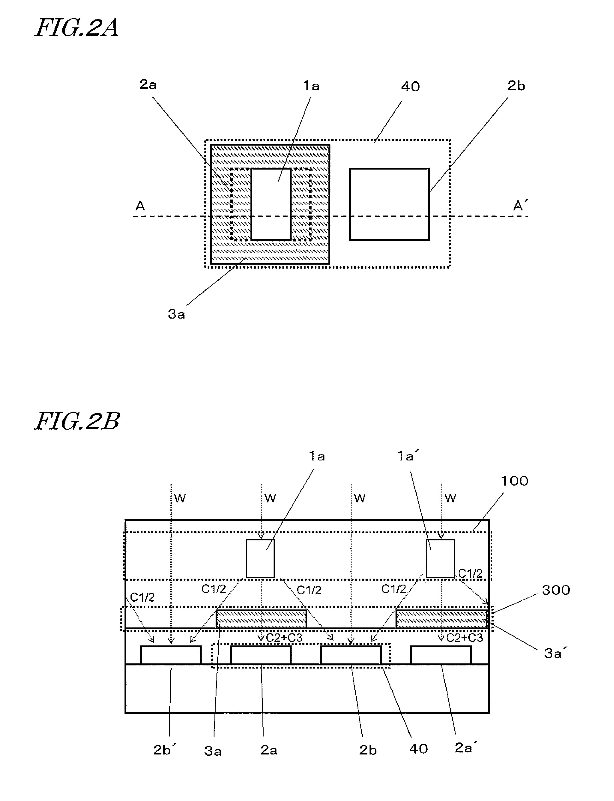
[0125]FIG. 11A is a plan view illustrating the basic structure of the image sensor 10 of this preferred embodiment. In each unit block 40, two dispersing elements 1a and 1d are arranged so as to respectively face two 2a and 2d out of the four photosensitive cells 2a, 2b, 2c and 2d. The dispersing elements 1a and 1d have the same property as the dispersing elements 1a and 1d of the first preferred embodiment described above. A color filter (Ye filter) 3a, w...

embodiment 3

[0139]Next, a third specific preferred embodiment of the present invention will be described with reference to FIGS. 12A through 12C. The image capture device of this preferred embodiment has the same configuration as the counterpart of the first preferred embodiment described above except the structure of the image sensor 10. Thus, the following description of this third preferred embodiment will be focused on only the difference from the first preferred embodiment and description of their common features will be omitted herein.

[0140]FIG. 12A is a plan view illustrating the basic structure of the image sensor 10 of this preferred embodiment. In each unit block 40, three dispersing elements 1b, 1cc and 1d are arranged so as to respectively face three 2b, 2c and 2d out of the four photosensitive cells 2a, 2b, 2c and 2d. The dispersing elements 1b and 1d have the same property as the dispersing elements 1b and 1d of the first preferred embodiment described above. The dispersing elemen...


PUM


Abstract

The solid-state image sensor of the present invention includes an array of photosensitive cells, an array 100 of dispersing elements, and an array 300 of color filters. The photosensitive cell array 200 has a number of unit blocks 40, each of which includes photosensitive cells 2a and 2b. The dispersing element array 100 includes a dispersing element 1a, which makes all of incoming light (W) but a light ray falling within a first wavelength range incident on the first photosensitive cell 2a and which also makes at least a part of the light ray falling within the first wavelength range incident on the second photosensitive cell 2b. A color filter 3a that either absorbs or reflects the light ray falling within the first wavelength range is arranged between the photosensitive cell 2a and the dispersing element 1a.

Description

TECHNICAL FIELD[0001]The present invention relates to a technique for increasing the sensitivity of a solid-state image sensor and realizing color representation using such a solid-state image sensor.BACKGROUND ART[0002]Recently, the performance and functionality of digital cameras and digital movie cameras that use some solid-state image sensor such as a CCD and a CMOS (which will be simply referred to herein as an “image sensor”) have been enhanced to an astonishing degree. In particular, the size of a pixel structure for use in an image sensor has been further reduced these days thanks to rapid development of semiconductor device processing technologies, thus getting an even greater number of pixels and drivers integrated together in an image sensor. And the performance of image sensors has been further enhanced as well. Meanwhile, cameras that use a backside illumination type image sensor, which receives incoming light on its back surface side, not on its principal surface side ...

Claims


Application Information

Patent Timeline
Patent Type & Authority Applications(United States)
IPC IPC(8): H04N5/335
CPCH01L27/14621H04N9/045H01L27/14629H01L27/14627H04N25/11H04N23/10
Inventor HIRAMOTO, MASAOSUZUKI, MASAAKI
Owner SOVEREIGN PEAK VENTURES LLC
Why Eureka
Try Eureka