Flip chip assembly method employing post-contact differential heating

a chip and differential heating technology, applied in the direction of welding/cutting media/materials, manufacturing tools, soldering apparatus, etc., can solve the problems of c4 balls or any other type of solder balls, semiconductor chip(s) to fail during the connection, and the problem of mechanical stress caused by the mismatch between cte's is exacerbated, so as to improve the integrity of the solder joint

Inactive Publication Date: 2012-08-30
IBM CORP
View PDF7 Cites 22 Cited by
  • Summary
  • Abstract
  • Description
  • Claims
  • Application Information

AI Technical Summary

Benefits of technology

[0008]A first substrate mounted to a bonder head and a second substrate mounted to a base plate are held at different elevated temperatures at the time of bonding that provide a substantially matched thermal expansion between the second substrate and the first substrate relative to room temperature. Further, the temperature of the solder material portions and the second substrate is raised at least up to the melting temperature after contact. The distance between the first substrate and the second substrate can be modulated to enhance the integrity of solder joints. Once the distance is at an optimum, the bonder head is detached, and the bonded structure is allowed to cool to form a bonded flip chip structure. Alternately, the bonder head can control the cooling rate of solder joints by being attached to the chip during cooling step.

Problems solved by technology

Connections employing an array of solder material portions, such as C4 balls or any other type of solder balls, are susceptible to mechanical stress created by a mismatch in the coefficients of thermal expansion (CTE's) between the semiconductor chip and the other semiconductor chip or the packaging substrate.
Such mechanical stress may cause cracks in the solder material portions, back-end-of-lines in chips, or the semiconductor chip(s), causing the semiconductor chip(s) to fail during flip chip assembly process and / or usage.
The problem of mechanical stress caused by the mismatch between CTE's are exacerbated when an organic substrate is employed for a packaging substrate because the mismatch of CTE's is greater between organic substrates and semiconductor substrates than between ceramic substrates and semiconductor substrates.
When an organic substrate is used as a packaging substrate for a fine pitch flip chip assembly, substrate warpage can occur in the conventional reflow process during which solder balls reflow.
This warpage can result in non-wetting of solder bumps and / or bridging between solder bumps, thereby decreasing the assembly yield.
Thermally-induced stress and strain in the flip-chip structure during a reflow process often results in a failure of back-end-of-line (BEOL) interconnect structures.
Warpage of organic substrates and thermally-induced stress and strain increase as the size of an organic substrate increases, which is common for high performance chips and components.
As a result, reflow of solder joint is non-existent or limited in this method.
Further, this method does not provide a mechanism for overcoming solder non-wet issues and solder bridging problems due to solder height variation in the array of solder material portions and in any other conductive bonding structure contacting the array of solder material portions, and substrate warpage.
Organic substrates always have a certain amount of initial warpage even at room temperature due to stacking of multi-layers of metals and polymers.

Method used


Image

  • Flip chip assembly method employing post-contact differential heating
  • Flip chip assembly method employing post-contact differential heating
  • Flip chip assembly method employing post-contact differential heating

Examples


second embodiment

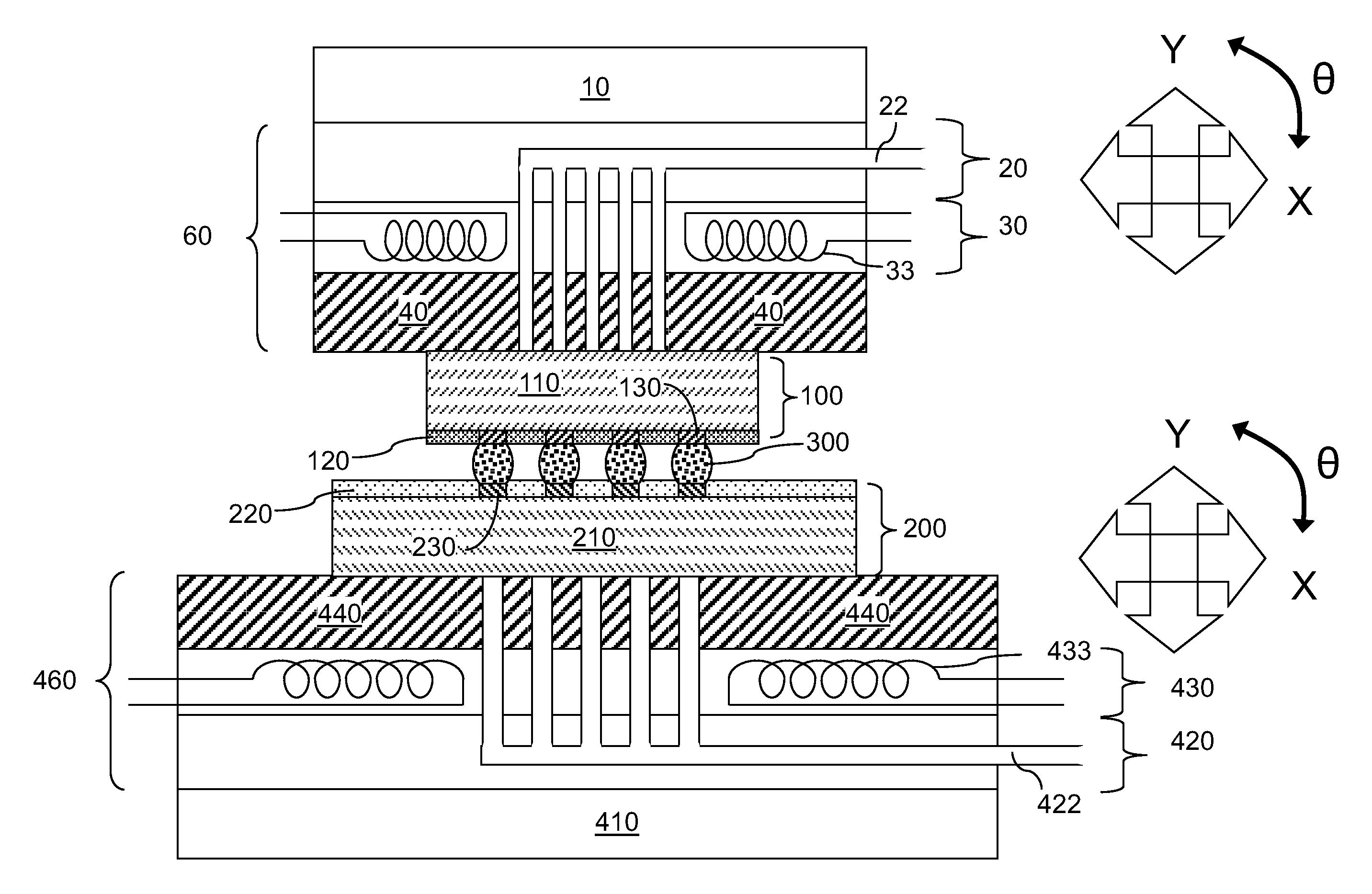
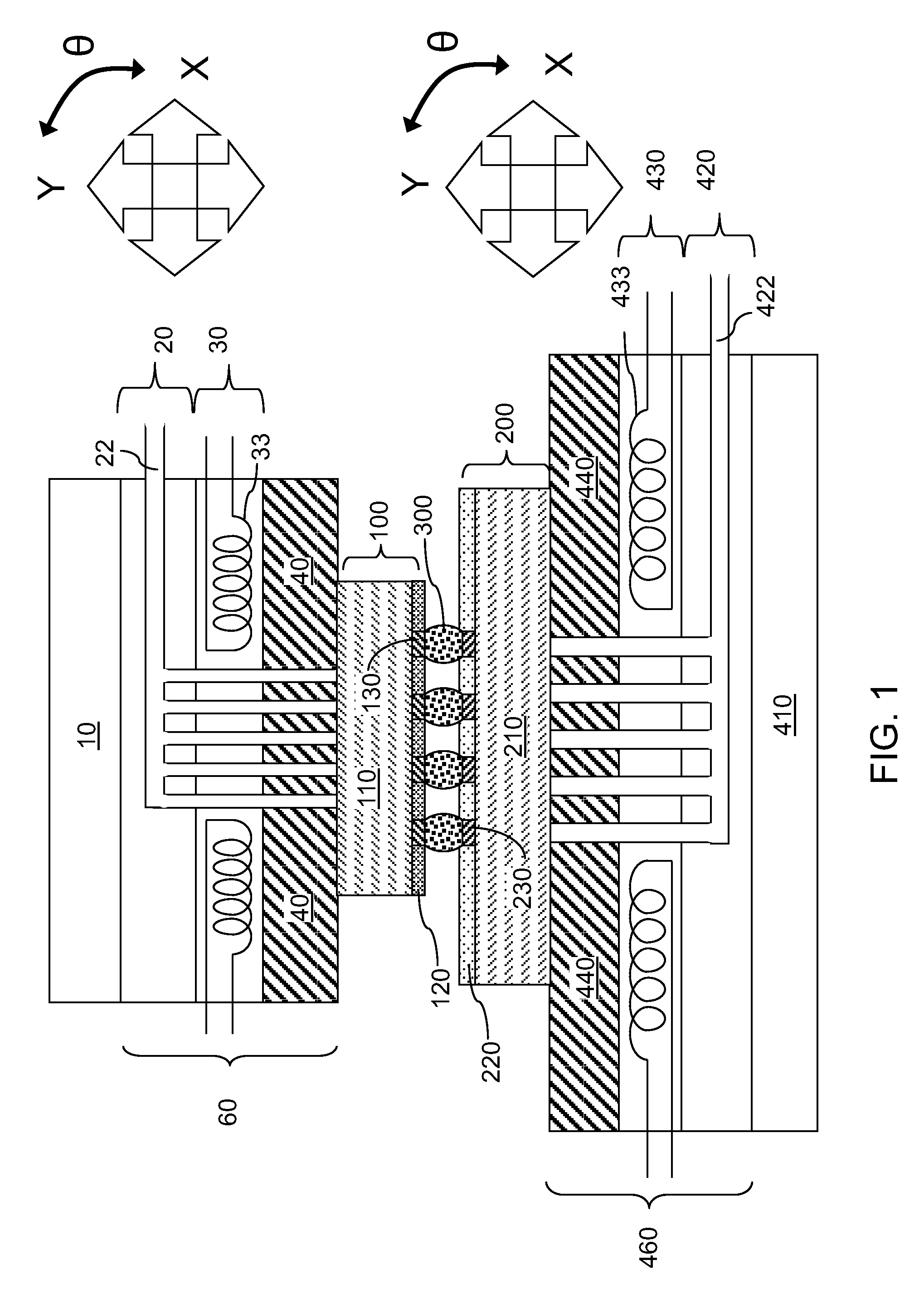
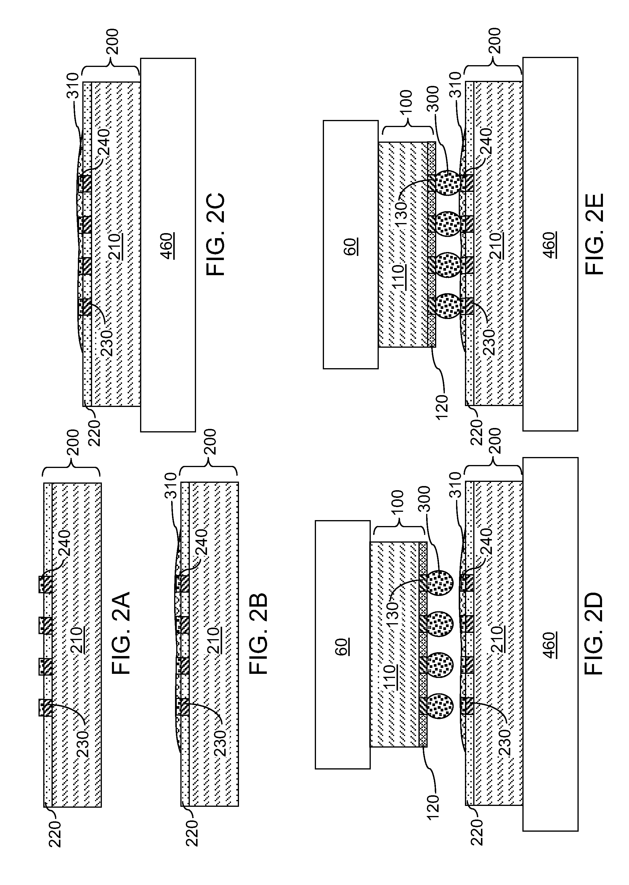
[0075]In the second embodiment, the second substrate 200 includes an array of metal structures such as an array of second bonding pads 230. The array of solder material portions 300 is bonded to the array of second bonding pads 230. The flux 310 may be optionally applied around the array of solder material portions 300 thereafter.

[0076]The first substrate 100 includes an array of metal pillars 330 and includes a metallic material such as copper. In one case, the array of metal pillars 330 can be an array of copper pillars consisting substantially of copper. The array of metal pillars 330 protrudes out of the surface of a first substrate 100, which is a bottom surface of the first substrate 100 while the first substrate 100 is held upside down.

first embodiment

[0077]The first substrate 100 is held at the second temperature, and the second substrate 200 is held at the first temperature employing the same temperature control schemes as in the

[0078]The processing steps of FIGS. 2E, 2F, and 2G are subsequently performed to form the second exemplary structure illustrated in FIG. 3B. At this step, the distance between the first substrate 100 and the second substrate 200 is decreased below the bonding distance.

[0079]In the second embodiment, the array of solder material portions 300 is bonded to the array of metal pillars 330 when the array of solder material portions 300 is brought into physical contact with the second substrate 200. The array of solder material portions 300 contacts sidewalls of the array of metal pillars after the array of solder material portions is brought into physical contact with the second substrate 200. The temperature of the first substrate 100 is maintained at the third temperature at this step as in the first embodi...

third embodiment

[0083]In the third embodiment, the array of solder material portions 300 can be bonded to an array of metal structures located on the one of the two substrates. FIG. 4A illustrates a case in which the array of solder balls 300 is bonded to the first substrate 100 before the first substrate 100 is heated to the second temperature. In this case, the array of solder balls 300 can be bonded to the array of first bonding pads 130. The second substrate 200 may, or may not, not include a second surface dielectric layer 220. The first substrate 100 includes a first array of metal structures such as an array of second bonding pads 130. A flux is not required in this embodiment, but may optionally be employed.

[0084]A first array of metal structures (such as bonding pads or metal pillars) is located on the first substrate 100, and a second array of metal structures 430 is located on the second substrate 200. In general, the array of solder material portions 300 is bonded to one of the first su...


PUM

PropertyMeasurementUnit
melting temperatureaaaaaaaaaa
temperatureaaaaaaaaaa

Abstract

A first substrate mounted to a bonder head and a second substrate mounted to a base plate are held at different elevated temperatures at the time of bonding that provide a substantially matched thermal expansion between the second substrate and the first substrate relative to room temperature. Further, the temperature of the solder material portions and the second substrate is raised at least up to the melting temperature after contact. The distance between the first substrate and the second substrate can be modulated to enhance the integrity of solder joints. Once the distance is at an optimum, the bonder head is detached, and the bonded structure is allowed to cool to form a bonded flip chip structure. Alternately, the bonder head can control the cooling rate of solder joints by being attached to the chip during cooling step.

Description

BACKGROUND[0001]The present disclosure relates to a method for bonding substrates, and particularly, to a method of bonding substrates while minimizing stress induced by a mismatch in the coefficients of thermal expansion (CTE's) between the substrates.[0002]A first substrate can be bonded to a second substrate by employing an array of solder material portions. For example, in a solder bonding employing bonding pads, each solder material portion contacts a bonding pad on the semiconductor chip and another bonding pad on another semiconductor chip or the packaging substrate. Each bonding pad is a contiguous metal pad typically formed out of the last metal layer of a metal interconnect structure during a semiconductor manufacturing sequence. Each bonding pad is large enough to accommodate the bottom portion of a solder material portion. Typically, an array of solder material portions can be employed to provide input / output (I / O) connections between the semiconductor chip and another s...

Claims


Application Information

Patent Timeline
Patent Type & Authority Applications(United States)
IPC IPC(8): B23K31/02B23K1/20
CPCB23K1/0016
Inventor KUMAR, RAJNEESHNAH, JAE-WOONGPERFECTO, ERIC D.
Owner IBM CORP
Why Eureka
Try Eureka