Image capture lens module and wafer level packaged image capture devices

a technology of image capture and lens module, which is applied in the direction of instruments, semiconductor devices, optics, etc., can solve the problems of high production volume, constant price erosion, and extremely difficult design and manufacturing of camera modules for portable electronic products

Active Publication Date: 2012-08-30
VISERA TECH CO LTD +1
View PDF6 Cites 20 Cited by
  • Summary
  • Abstract
  • Description
  • Claims
  • Application Information

AI Technical Summary

Benefits of technology

[0008]Embodiments of the invention provide an image capture lens module, comprising: a compound lens with a first lens element and a second lens element molded on both sides of a wafer level substrate; and a field stop disposed at an interface between the first lens element and the wafer level substrate or at an interface between the second lens element and the wafer level substrate, wherein the field stop is a coating layer with a polygonal transparent area corresponding to an effective sensing area.
[0009]Embodiments of the invention further provide an image capture lens module, comprising: a first compound lens with a first lens element and a second lens element molded on both sides of a first wafer level substrate; a second compound lens with a third lens element and a fourth lens element molded on both sides of a second wafer level substrate; a field stop disposed at an interface between the first lens element and the first wafer level substrate, or at an interface between the second lens element and the first wafer level substrate, or at an interface between the third lens element and the second wafer level substrate, or at an interface between the fourth lens element and the second wafer level substrate; and a spacer interposed between the first and second compound lenses to separate the first and second compound lenses with a predetermined gap, wherein the field stop is a coating layer with a polygonal transparent area corresponding to an effective sensing area.
[0010]Embodiments of the invention further provide a wafer level packaged image capture device, comprising: an aperture; a first compound lens with a first lens element and a second lens element molded on both sides of a first wafer level substrate; a second compound lens with a third lens element and a fourth lens element molded on both sides of a second wafer level substrate; a field stop disposed at an interface between the first lens element and the first wafer level substrate, or at an interface between the second lens element and the first wafer level substrate, or at an interface between the third lens element and the second wafer level substrate, or at an interface between the fourth lens element and the second wafer level substrate; and a spacer interposed between the first and second compound lenses to separate the first and second compound lenses with a predetermined gap; and a cover glass for an image sensor positioned behind the second compound lens, wherein the aperture, the first compound lens, the second compound lens and the cover glass are arranged in sequence from an object side to an image side, and the field stop is a coating layer with a polygonal transparent area corresponding to an effective sensing area.

Problems solved by technology

The design and manufacturing of camera modules for portable electronic products is extremely challenging.
Some pervasive factors include: high production volume, constant price erosion, size limitations and changing performance and functionality requirements.
There are, however, some problems for the conventional image capture lens module, such as inner light scattering, stray-light effect and ghost images.
Particularly, the inner circular area of the plastic or metal field stop is larger than the effective sensing area of the image plane, resulting in multiple light reflections inside of the lens module.
These multiple light reflections may result in ghost images and stray-light.

Method used


Image

  • Image capture lens module and wafer level packaged image capture devices
  • Image capture lens module and wafer level packaged image capture devices
  • Image capture lens module and wafer level packaged image capture devices

Examples


Embodiment Construction

[0016]The following description is of the best-contemplated mode of carrying out the invention. This description is made for the purpose of illustrating the general principles of the invention and should not be taken in a limiting sense. The scope of the invention is best determined by reference to the appended claims.

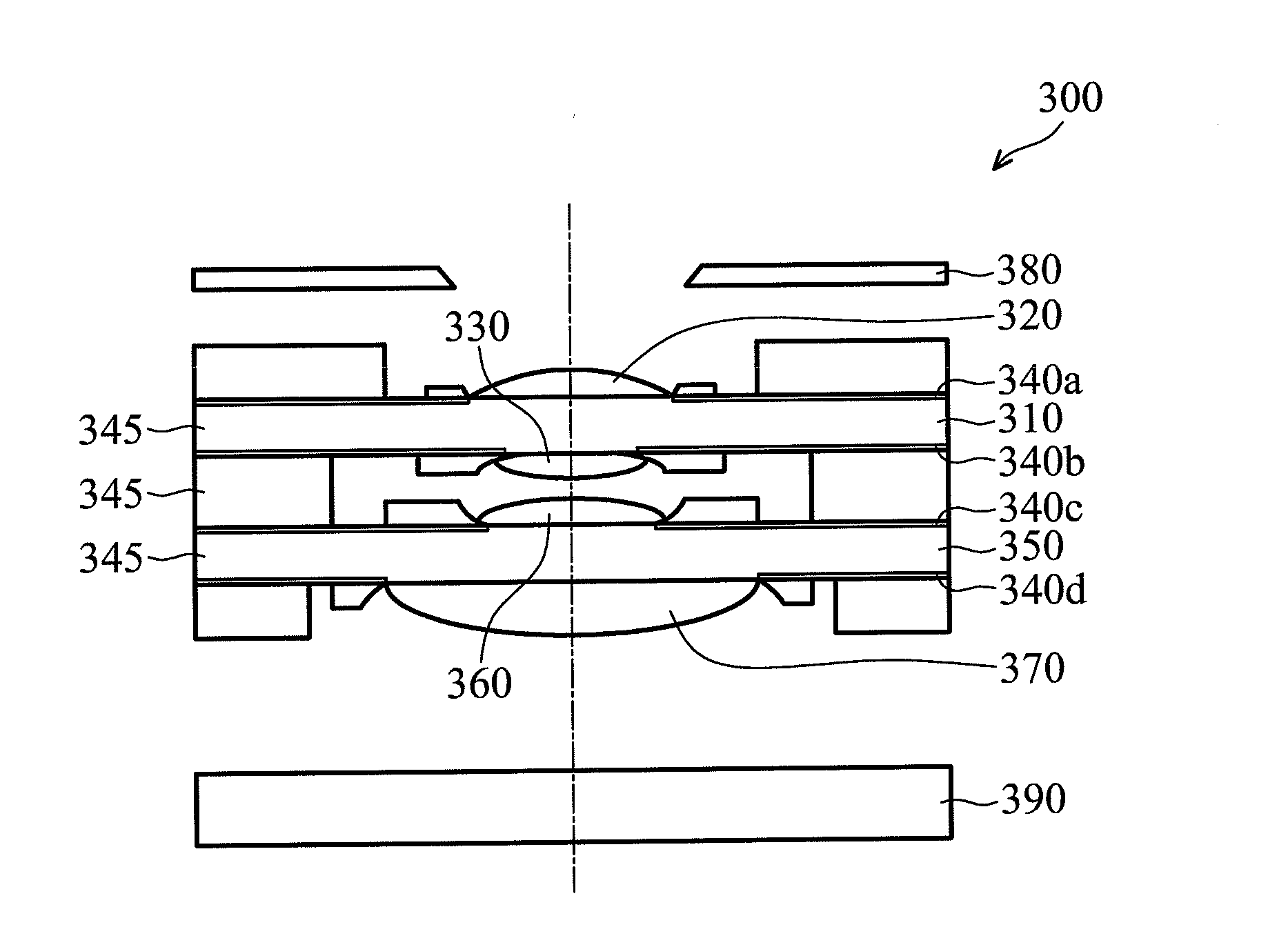
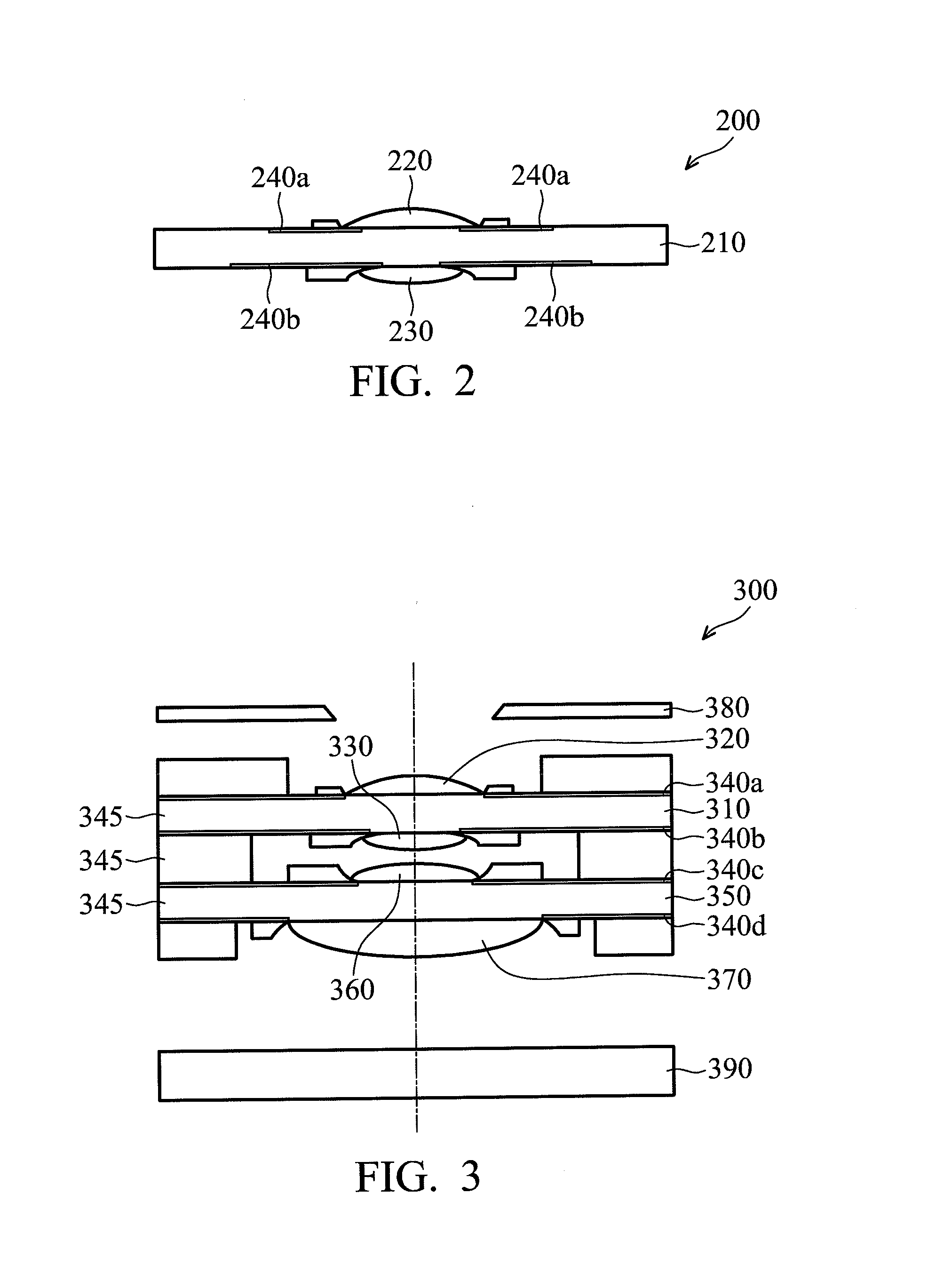
[0017]Embodiments of the invention provide high performance wafer-level packages with image capture lens modules and CMOS sensors preventing ghost images and stray-light. An image capture device of an embodiment of the invention is made up of an image capture lens module associated with an image sensor. This association enables selecting a particular zone in space, eliminating the rest and optimizing the flux collecting capability of the image sensor. The image capture lens module controls incident rays by stops. For instance, an aperture stop confines the cross sectional area of the bundle of rays from object to image point, thereby controlling the brightness of the i...


PUM


Abstract

Image capture lens modules and wafer level packaged image capture devices are presented. The image capture lens module includes a compound lens with a first lens element and a second lens element molded on both sides of a substrate, and a field stop disposed at an interface between the first lens element and the substrate or at an interface between the second lens element and the substrate, wherein the field stop is a coating layer with a polygonal transparent area.

Description

BACKGROUND OF THE INVENTION[0001]1. Field of the Invention[0002]The invention relates to image capture lens modules, and more particularly to, high performance wafer-level packaged image capture lens modules and wafer level packaged image capture devices.[0003]2. Description of the Related Art[0004]Digital cameras utilizing high-resolution electronic imaging sensors typically require high resolution optical components such as image capture lens modules. The design and manufacturing of camera modules for portable electronic products is extremely challenging. Some pervasive factors include: high production volume, constant price erosion, size limitations and changing performance and functionality requirements.[0005]The number of image capture lenses on a digital camera module that focus a scene onto an imager can be as few as one for a digital camera module, or as many as four for a digital camera module with mega pixel resolution. Usually, the lenses are plastic, to lower costs. Howe...

Claims


Application Information

Patent Timeline
Patent Type & Authority Applications(United States)
IPC IPC(8): G02B13/18
CPCG02B9/02G02B9/08G02B9/04G02B13/003G02B13/004G02B13/0085H01L27/14618G02B5/005H01L2924/0002H01L2924/00
Inventor LIN, CHUN-CHIDENG, JAU-JANCHEN, WEI-PING
Owner VISERA TECH CO LTD
Why Eureka
Try Eureka