

Solid-state imaging device, method of manufacturing solid-state imaging device, and electronic apparatus
A technology of a solid-state imaging device and a manufacturing method, which is applied in the direction of electric solid-state devices, solid-state image signal generators, semiconductor devices, etc., can solve problems such as the inability to bear the stress of SiN films, the expansion and contraction of propylene thermoplastic resins, etc., and achieve improved sensitivity characteristics, high The effect of sensitivity
Active Publication Date: 2012-05-09
SONY SEMICON SOLUTIONS CORP
View PDF8 Cites 21 Cited by
- Summary
- Abstract
- Description
- Claims
- Application Information
AI Technical Summary
Problems solved by technology
In this state, when an antireflection film composed of, for example, a SiN film is formed on the surface of the microlens, the acrylic thermoplastic resin as the color filter cover film may not be able to withstand the stress of the SiN film, and the acrylic thermoplastic resin may Stretch phenomenon
Method used
View moreImage
Smart ImageViewing Examples

Examples
no. 1 example
[0054] 1. First Embodiment (Example of structure and manufacturing method of solid-state imaging device)
no. 2 example
[0055] 2. Second Embodiment (Example of structure and manufacturing method of solid-state imaging device)
no. 3 example
[0056] 3. Third Embodiment (Example of structure and manufacturing method of solid-state imaging device)
Login to View More PUM
 Abstract
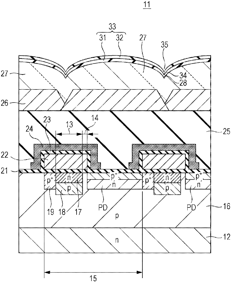
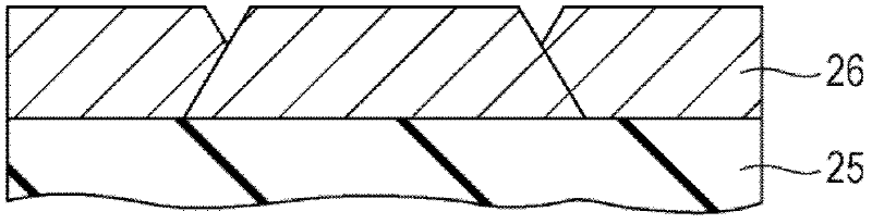
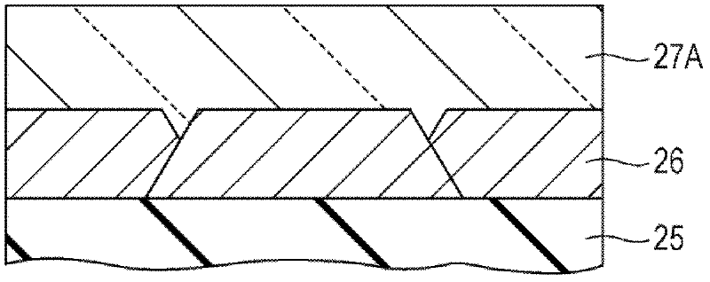
The invention discloses a solid-state imaging device, a method of manufacturing the solid-state imaging device, and an electronic apparatus. The solid-state imaging device includes a plurality of pixels formed on a semiconductor substrate and include a photoelectric conversion unit; a color filter on the pixels; an on-chip microlens made of an organic film on the color filter, corresponding to each of the pixels; a first inorganic film formed on a surface of the on-chip microlens and having a higher refraction index than the on-chip microlens; and a second inorganic film formed on a surface of the first inorganic film and having a lower refraction index than the on-chip microlens and the first inorganic film, in which at least the second inorganic film includes a non-lens area at an interface of an adjacent second inorganic film. The solid-state imaging device, the method of manufacturing the solid-state imaging device, and the electronic apparatus can improve image quality and sensitivity characteristic.
Description
[0001] Cross reference of related applications [0002] This application contains the subject matter related to the disclosure of the Japanese priority patent application JP 2010-227755 filed with the Japan Patent Office on October 7, 2010, and the entire content of the priority patent application is hereby incorporated by reference. . Technical field [0003] The present invention relates to a solid-state imaging device, a method of manufacturing the solid-state imaging device, and an electronic device such as a camera equipped with the solid-state imaging device. Background technique [0004] As a solid-state imaging device (image sensor), a CMOS solid-state imaging device or a CCD solid-state imaging device has been proposed. Solid-state imaging devices have been used in digital cameras, digital video cameras, and various portable terminal devices (for example, mobile phones equipped with cameras, etc.). The CMOS solid-state imaging device has a lower power supply voltage than ...
Claims
Login to View More Application Information
Patent Timeline
 Patent Type & AuthorityApplications(China)
IPC IPC(8): H01L27/146H04N5/225H04N23/12
CPCH01L27/14621H01L27/14843H01L27/14685H01L27/14627H04N9/045H01L27/14818H01L27/14623H04N23/10H01L27/148
Inventor大塚洋一荻野明子田渕清隆谷国敬理
OwnerSONY SEMICON SOLUTIONS CORP