Polymorphic Stacked DRAM Memory Architecture

a stacked, memory architecture technology, applied in the direction of memory adressing/allocation/relocation, digital storage, instruments, etc., can solve the problems of limited scalability, limited dram memory on the chip, and significant performance limitations created, so as to achieve less overhead of space, improve scalability, and facilitate access time

Inactive Publication Date: 2012-08-30
ADVANCED MICRO DEVICES INC
View PDF8 Cites 63 Cited by
  • Summary
  • Abstract
  • Description
  • Claims
  • Application Information

AI Technical Summary

Problems solved by technology

With today's high performance multi-core devices, there can be significant performance limitations created when multiple cores request read / write access to off-chip DRAM memory over limited bandwidth I / O pins which have limited scalability.
Off-chip DRAM memory is also limited by the lack of scalability in the DIMM slots per channel.
However, the addition of a large storage memory area in the stacked memory presents storage management challenges for efficiently using the additional memory and preventing performance losses or costs associated with stacked memories, depending on whether the stacked memories operate as memories or caches.

Method used


Image

  • Polymorphic Stacked DRAM Memory Architecture
  • Polymorphic Stacked DRAM Memory Architecture
  • Polymorphic Stacked DRAM Memory Architecture

Examples


Embodiment Construction

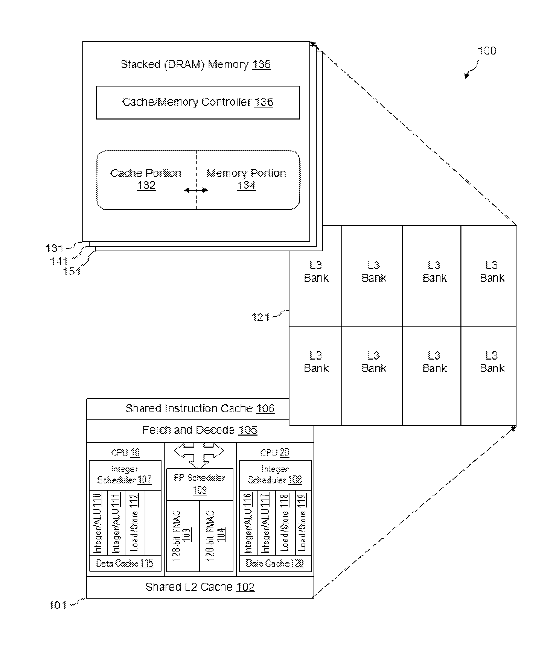
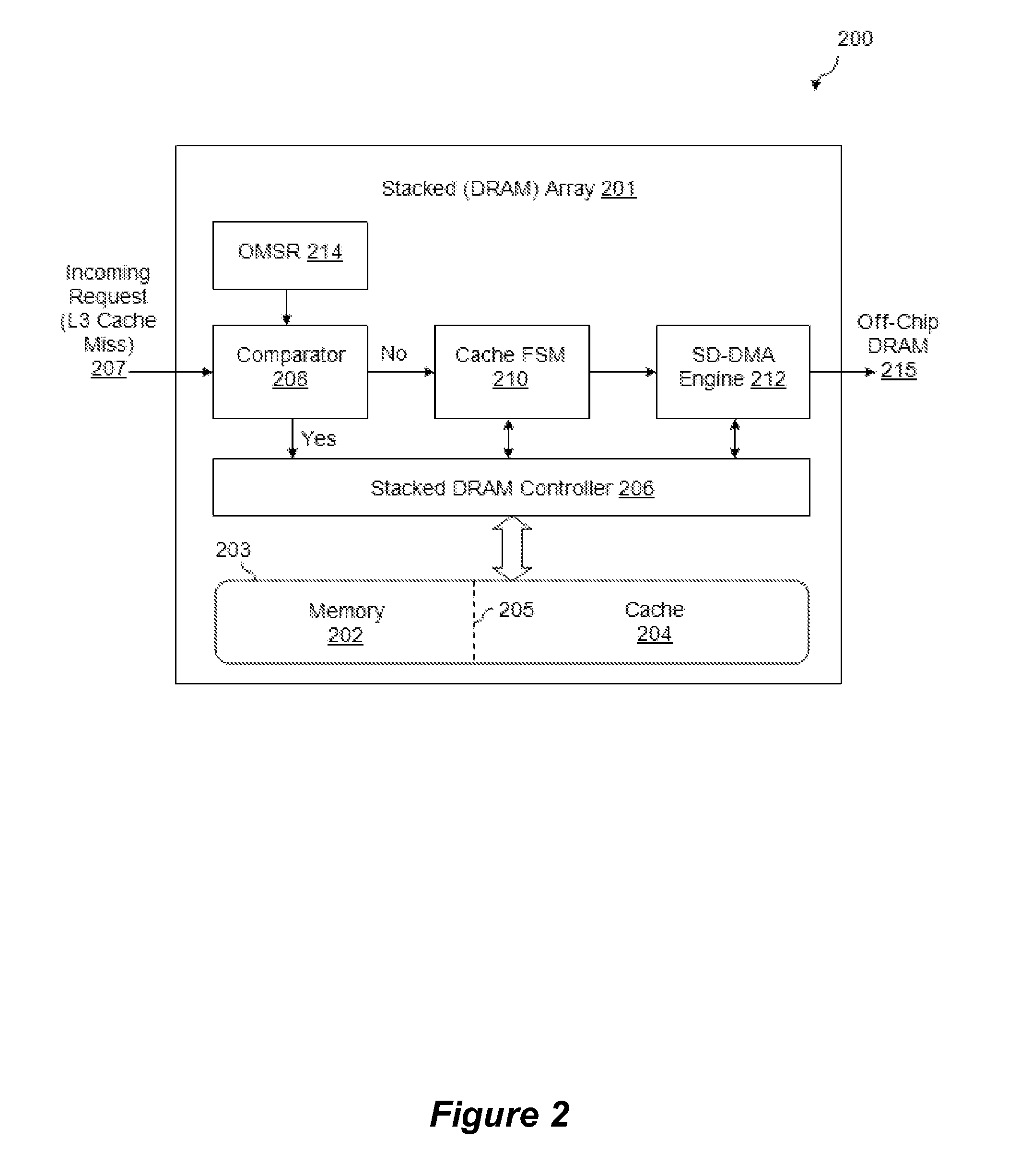
[0006]Broadly speaking, embodiments of the present invention provide a polymorphic stacked DRAM architecture, circuit, system, and method of operation wherein the stacked DRAM may be dynamically configured to operate part of the stacked DRAM as memory and part of the stacked DRAM as cache. The memory portion of the stacked DRAM is specified with reference to a predetermined region of the physical address space so that data accesses to and from the memory portion corresponds to merely reading or writing to those locations. The cache portion of the stacked DRAM is specified with reference to a Finite State Machine (FSM) which checks the address tags to identify if the required data is in the cache portion and enables reads / writes based on that information. With the disclosed polymorphic stacked DRAM, the partition sizes between the memory and cache portions may vary dynamically based on application requirements. By optimally splitting the stacked DRAM between memory and cache portions...


PUM


Abstract

A 3D stacked processor device is described which includes a processor chip and a stacked polymorphic DRAM memory chip connected to the processor chip through a plurality of through-silicon-via structures, where the stacked DRAM memory chip includes a memory with an adjustable memory portion and an adjustable cache portion such that memory can operate simultaneously in both memory and cache modes.

Description

BACKGROUND OF THE INVENTION[0001]1. Field of the Invention[0002]The present invention relates in general to integrated circuits. In one aspect, the present invention relates to a dynamic random access memory (DRAM) architecture and method for operating same.[0003]2. Description of the Related Art[0004]With today's high performance multi-core devices, there can be significant performance limitations created when multiple cores request read / write access to off-chip DRAM memory over limited bandwidth I / O pins which have limited scalability. Off-chip DRAM memory is also limited by the lack of scalability in the DIMM slots per channel. Data bandwidth can be improved with multi-dimensional stacking of memory on the processing element(s) which also reduces access latency, reduces energy and power requirements, and enables merging of different technologies (e.g., static random access memory and DRAM) on top of processing logic to increase storage sizes. However, the addition of a large stor...

Claims


Application Information

Patent Timeline
Patent Type & Authority Applications(United States)
IPC IPC(8): G06F12/06G06F12/08
CPCG11C5/02G11C7/1006G06F2212/6012G06F12/0893G11C2207/2245
Inventor CHUNG, JAEWOONGSOUNDARARAJAN, NIRANJAN
Owner ADVANCED MICRO DEVICES INC
Why Eureka
Try Eureka