6F2 access transistor arrangement and semiconductor memory device

a technology of access transistors and access transistors, which is applied in the direction of transistors, semiconductor devices, electrical appliances, etc., can solve the problems of high repetition rate, high repeat rate, and high leakage current of conventional isolation transistors to storage nodes, so as to reduce pattern process complexity, enhance isolation properties, and enhance isolation properties

Inactive Publication Date: 2006-12-14
POLARIS INNOVATIONS LTD
View PDF11 Cites 62 Cited by
  • Summary
  • Abstract
  • Description
  • Claims
  • Application Information

AI Technical Summary

Benefits of technology

[0025] Thus, access transistors and isolation transistor are formed as recessed channel transistors with enhanced insulation properties. Providing identical recess channel devices having enhanced isolation properties for both the access transistors and the isolation transistor eliminates the need for different processing of the transistor devices and reduces pattern process complexity. Only stripe-shaped masks with repetitive line patterns having a width / pitch ratio of about 1:2 are required facilitating a true 6F2 cell size for high packaging densities. Low dopant concentrations both for node contact sections and bit line contact sections of the access transistors become feasible resulting in further reduced node junction leakage current and reduced process complexity.

Problems solved by technology

Compared to insulating pits, conventional isolation transistors suffer from a higher leakage current to the storage node, such that the storage device is gradually discharged and a high repetition rate of a refresh cycle is necessary to restore data.
Due to the occurrence of short channel effects, for example excessive sub-threshold leakage current, planar isolation transistors do not scale down well to sub 100 nanometer technologies with a minimum feature size of photolithographic patterns of less than 100 nanometers.

Method used


Image

  • 6F2 access transistor arrangement and semiconductor memory device
  • 6F2 access transistor arrangement and semiconductor memory device
  • 6F2 access transistor arrangement and semiconductor memory device

Examples


first embodiment

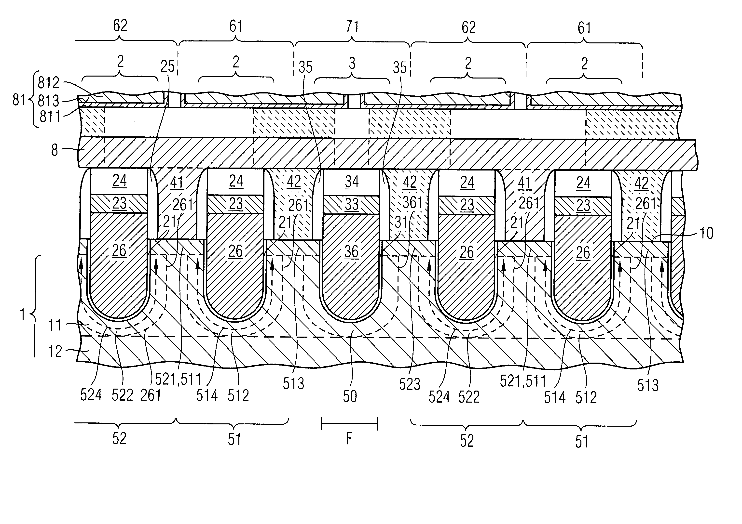
[0057]FIG. 2 is a cross-sectional view of an access transistor arrangement along cut line II of FIG. 4 according to the inventive access transistor arrangement.

[0058] The cut line of the cross-sectional view of FIG. 2 runs along a straight semiconductor line 11 extending outwardly from a bulk section 12 of a semiconductor substrate 1 which preferably consists of a single crystalline semiconductor, such as single crystalline silicon. In two parallel planes in front of and behind the cut plane the semiconductor lines 11 are confined by row insulator lines 9. The arrangement of the row insulator lines 9 follows from the corresponding plane view according to FIG. 4.

[0059] Each semiconductor line 11 comprises the active areas 51, 52 of pairs of access transistors 61, 62. Each active area 51, 52 comprises a bit line contact section 511, 521 and a node contact section 513, 523, wherein both the bit line contact section 511, 521 and the node contact section 513, 523 adjoin the pattern surf...

second embodiment

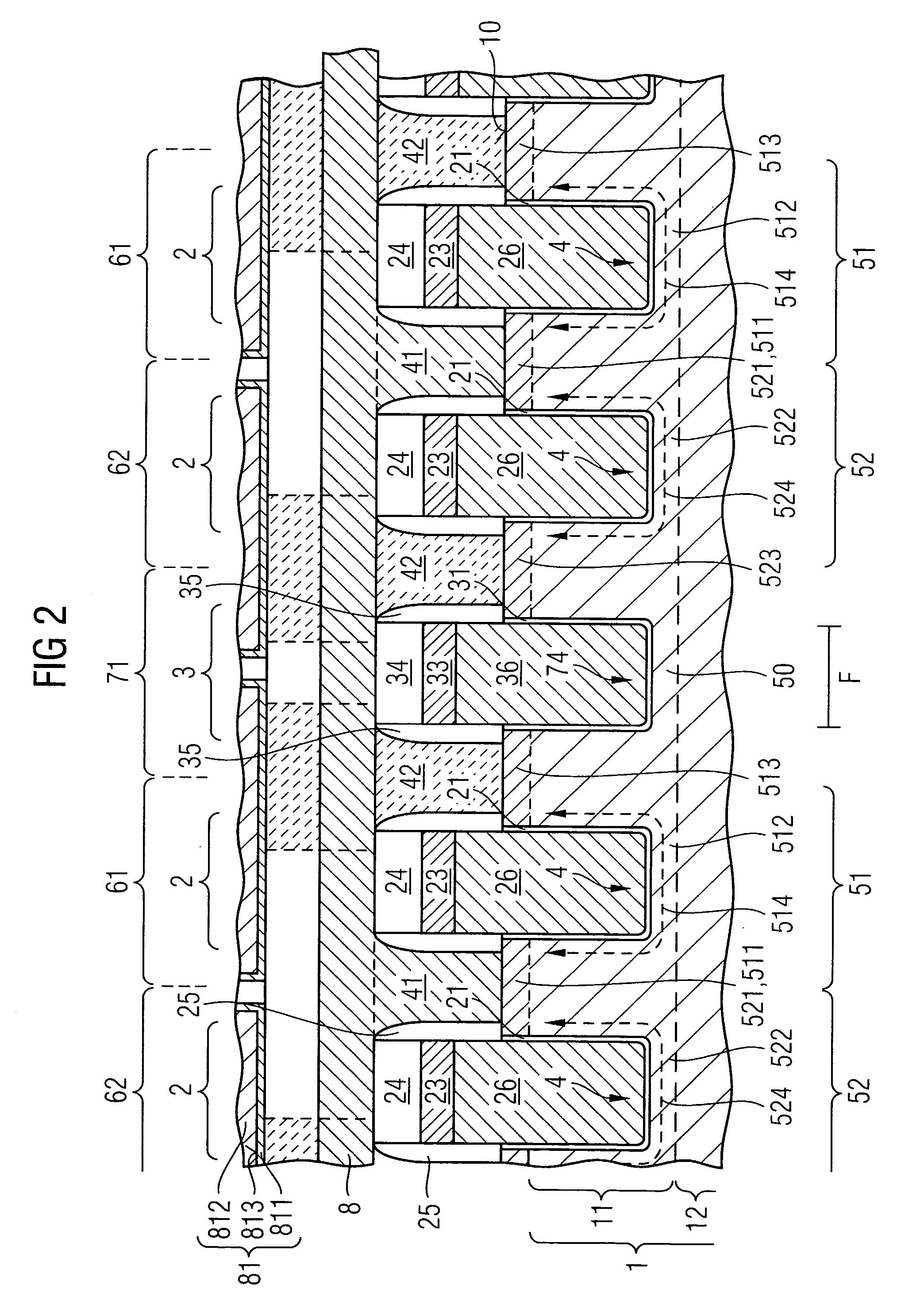
[0076]FIG. 3 is a cross-sectional view of an access transistor arrangement along cut line II of FIG. 4 according to the inventive access transistor arrangement.

[0077] The grooves 4, 74 of both the isolation 71 and the access transistors 61, 62 are formed U-shaped. With U-shaped grooves 4, 74, corner effects may be avoided, which may deteriorate the electrical properties of the transistors 61, 62, 71 as well as device reliability.

[0078] In other embodiments the partly buried semiconductor layers 26, 36 of the gate conductor lines 2, 3 may have extensions 261, 361 adjoining confining sections of the sidewalls of the active areas 51, such that charge carrier distribution in the channel sections 512, 522 as well as in the isolation areas 50 are controlled in a FinFET-like manner.

[0079]FIG. 4 is a simplified plan view of a section of an access transistor array in a shared bit line layout with straight semiconductor lines 11. The semiconductor lines 11 comprise active areas 51, 52. For ...


PUM


Abstract

An access transistor arrangement is provided for a 6F2 stacked capacitor DRAM memory cell layout with shared bit line contacts. The access transistors are arranged in pairs along semiconductor lines. The two transistors of each pair of transistors are arranged laterally reversed opposing the respective common bit line section. Each pair of access transistors is separated from the adjacent pair of access transistors by an isolation transistor which is permanently turned off. The access transistors and the isolation transistors are formed as identical recessed channel transistors with elongated channel and enhanced isolation properties. The same dopant concentration may be provided for both junctions of the access transistors. As identical devices are provided both as access transistor and as isolation transistors, the complexity of lithographic patterning processes is reduced.

Description

FIELD OF THE INVENTION [0001] The present invention relates to 6F2 access transistor arrays for semiconductor memory devices having bit lines and storage devices arranged above a pattern surface of a semiconductor substrate. The present invention relates further to a semiconductor memory device with 6F2 cell size. DESCRIPTION OF THE RELATED ART [0002] A semiconductor memory cell typically includes a storage device for storing data and an access device for accessing the data stored in the storage device. [0003] In DRAM memory cells, data is stored by charging or discharging a storage capacitor. In stacked capacitor type DRAM memory cells, the capacitors are placed on top of the access devices. Typically field-effect access transistors (FETs) are provided as access devices. [0004] Active areas of the access transistors are formed in a single crystalline semiconductor substrate. The active area comprises a first doped region defining a first source / drain-region, a second doped region d...

Claims


Application Information

Patent Timeline
Patent Type & Authority Applications(United States)
IPC IPC(8): H01L21/8242H01L27/108
CPCH01L21/76232H01L27/0207H01L27/10897H01L27/10888H01L27/10873H10B12/05H10B12/50H10B12/485
Inventor SCHLOESSER, TILL
Owner POLARIS INNOVATIONS LTD
Why Eureka
Try Eureka