

DRAM memory cell and array having pass transistors with surrounding gate
a memory cell and array technology, applied in the field of dynamic random access memory (dram) storage cells and arrays, can solve the problems of increasing the amount of memory required for systems, increasing the capacitance load on the word line, and not providing amplified bit line data as output data, etc., to achieve advantageous charge storage capabilities and greater control over the channel region
- Summary
- Abstract
- Description
- Claims
- Application Information
AI Technical Summary
Benefits of technology
Problems solved by technology
Method used
Image

Examples
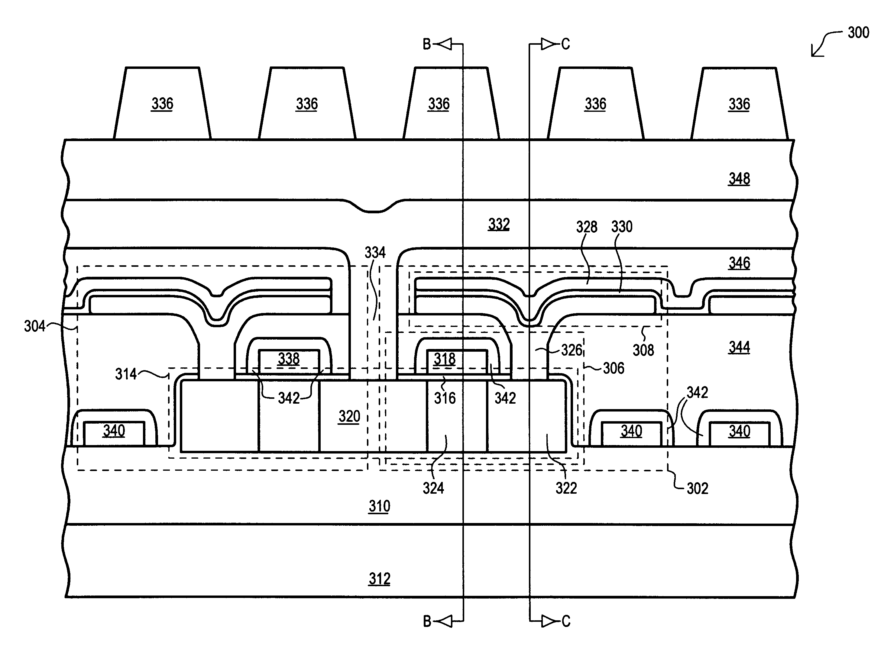
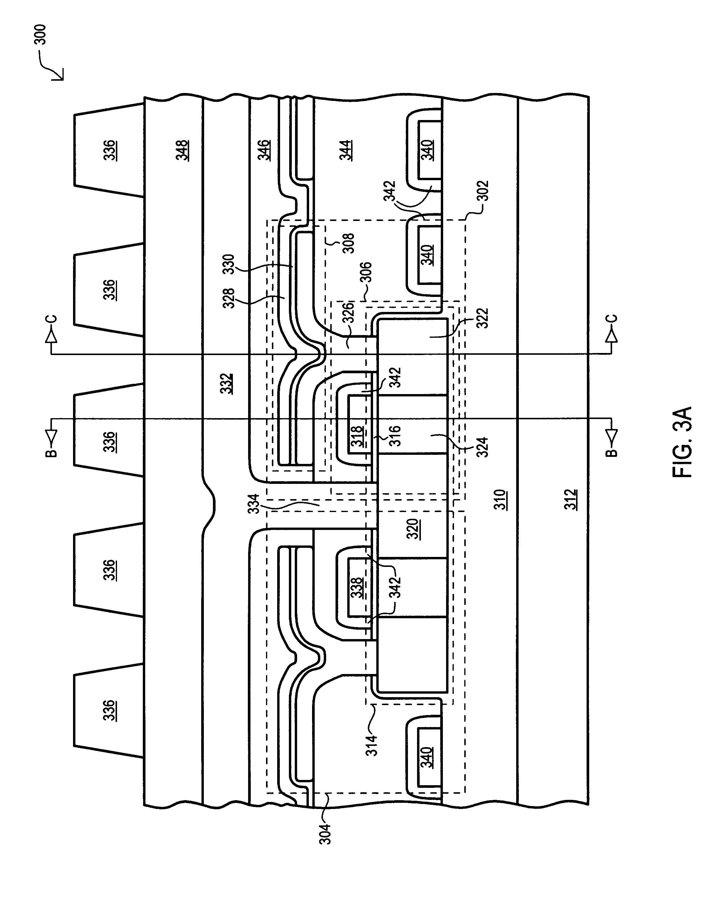
embodiment 300
Referring now to FIG. 3A, a portion of a preferred embodiment DRAM array is set forth in a side cross sectional view. The array is designated by the general reference character 300 and is formed using silicon-on-insulator (SOI) technology. The array 300 is shown to include a first memory cell and a second memory cell, show by the general reference characters 302 and 304, respectively. In the preferred embodiment 300, the second memory cell 304 mirrors the first memory cell 302, therefore only the constituents of the first memory cell 302 will be discussed in detail. The first memory cell 302 includes a pass transistor 306 and storage capacitor 308, both formed on a substrate insulator layer 310. The substrate insulator layer 310 is formed over a monocrystalline semiconductor substrate 312.
The pass transistor 306 is formed within one portion of a silicon mesa 314. A gate insulating layer 316 is disposed on the top surface of the silicon mesa 314, and a control gate 318 is formed on t...
first embodiment
In order to form the control gate 318, a polysilicon layer is deposited over the gate insulating layer 316. A pattern and etch step is then used to form the control gate 318 above the channel region 324. It is understood that, in the first embodiment memory cell 300, the control gate 318 extends along a portion of, or the entire length of, a memory cell array in the row direction. Thus, the control gate 318 can also be considered as a word line. At the same time control gate 318 is formed, a number of other control gates are also formed. The control gate for the second memory cell 304 is shown as 338. In addition, control gates for adjacent row pairs are shown as 340.
The preferred embodiment control gate arrangement is set forth in an isometric view in FIG. 5. FIG. 5 sets forth the same general view of FIG. 4, but following the formation of a gate insulating layer and the control gates. The silicon mesas are identified by the same reference numerals (402a-402e) as FIG. 4. The gate i...
embodiment 600
If reference is made to FIG. 8 in conjunction with FIGS. 3A-3C, the word line strap 800 of FIG. 8 corresponds to the word line straps 336 of FIGS. 3A and 3B. As such, in the preferred embodiment 600, the word line strap layer 800 is a metal, such as Al. The word line (WL) of FIG. 8 corresponds with the control gates (318, 338 and 340) of FIGS. 3A and 3B, and is formed from polysilicon. As was previously noted, the function of the word line strapping structure 612 is to reduce the effective resistance of the word lines.
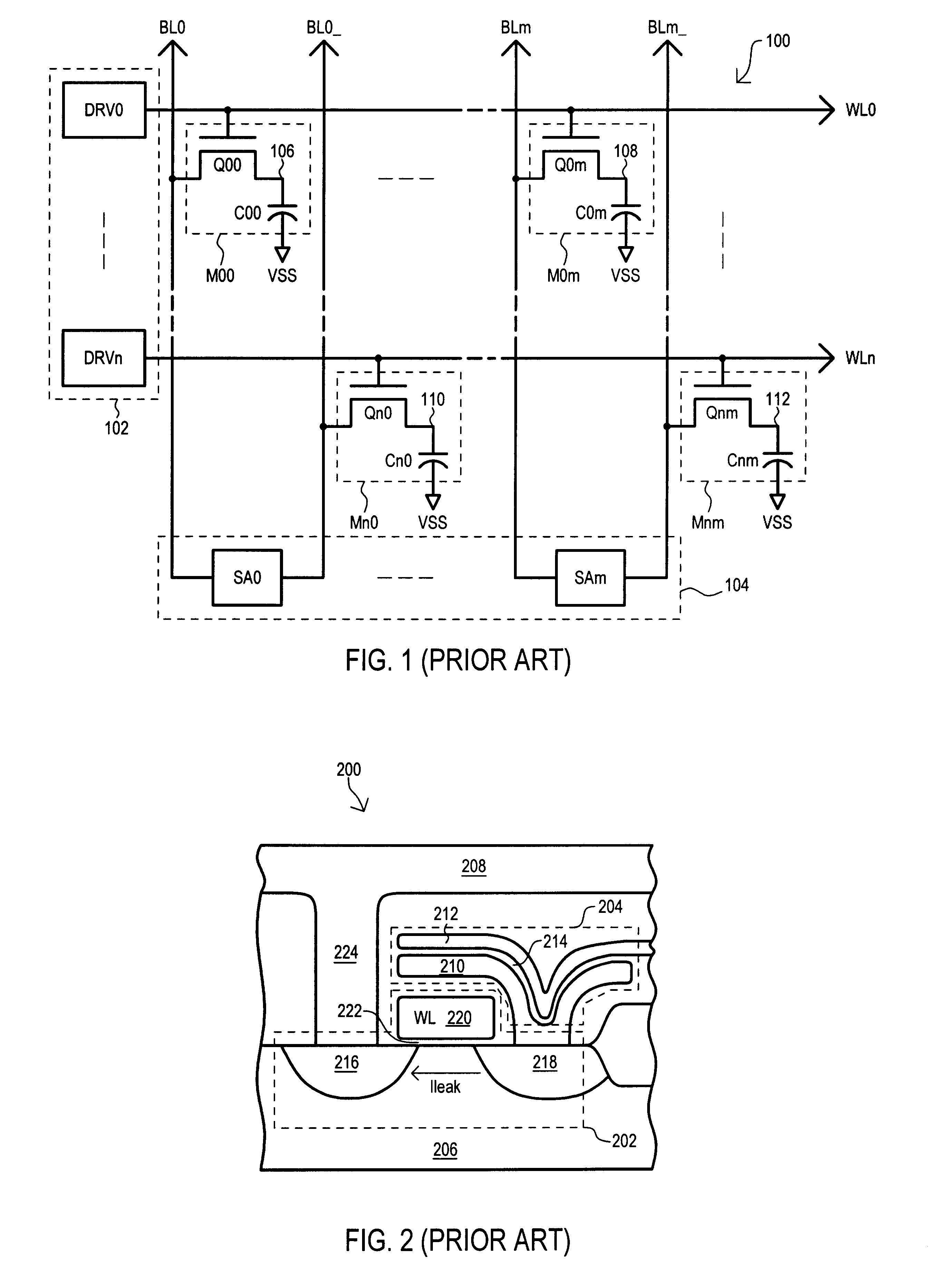
Referring once again to FIG. 6, the left sense amplifier section 604 and the right sense amplifier section 606 are shown to be disposed on opposite sides of the array 600. In order to access every memory cell 614 within array 600, it is necessary to have a sense amplifier for every pair of bit lines 610 in the memory array 600. Because there are two sense amplifier sections (604 and 606), half of the sense amplifiers are in the left sense amplifier section 604, and the...
PUM
 Abstract
Description
Claims
Application Information