

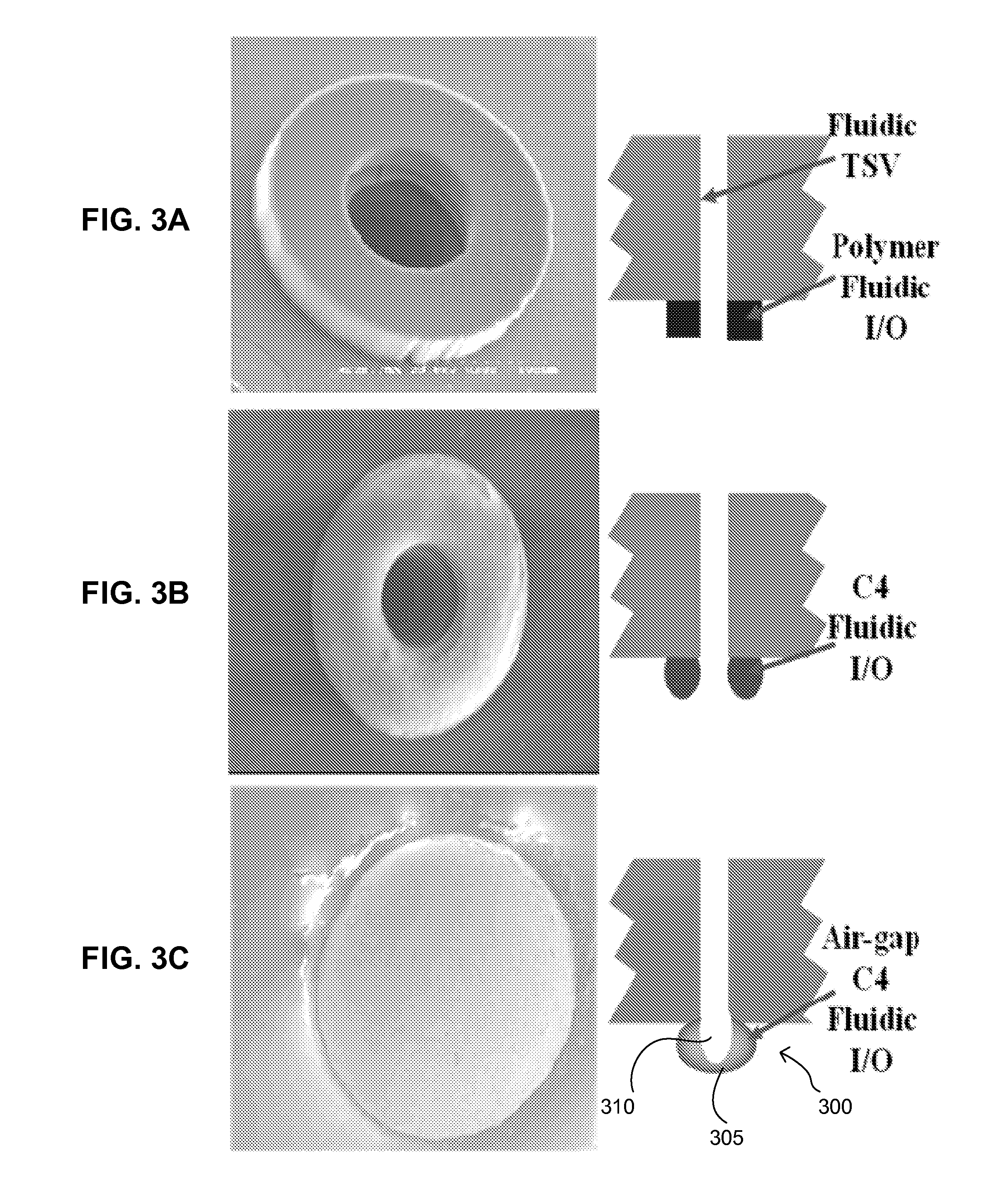
Air-gap c4 fluidic I/O interconnects and methods of fabricating same
a fluidic i/o interconnect and air gap technology, applied in the field of three-dimensional integrated circuits, can solve the problems of affecting device operation, affecting end user usage patterns, and the need to cool electronics and diminish device hot spots, and the need to reduce hot spots has never been greater
- Summary
- Abstract
- Description
- Claims
- Application Information
AI Technical Summary
Benefits of technology
Problems solved by technology
Method used
Image

Examples
Embodiment Construction
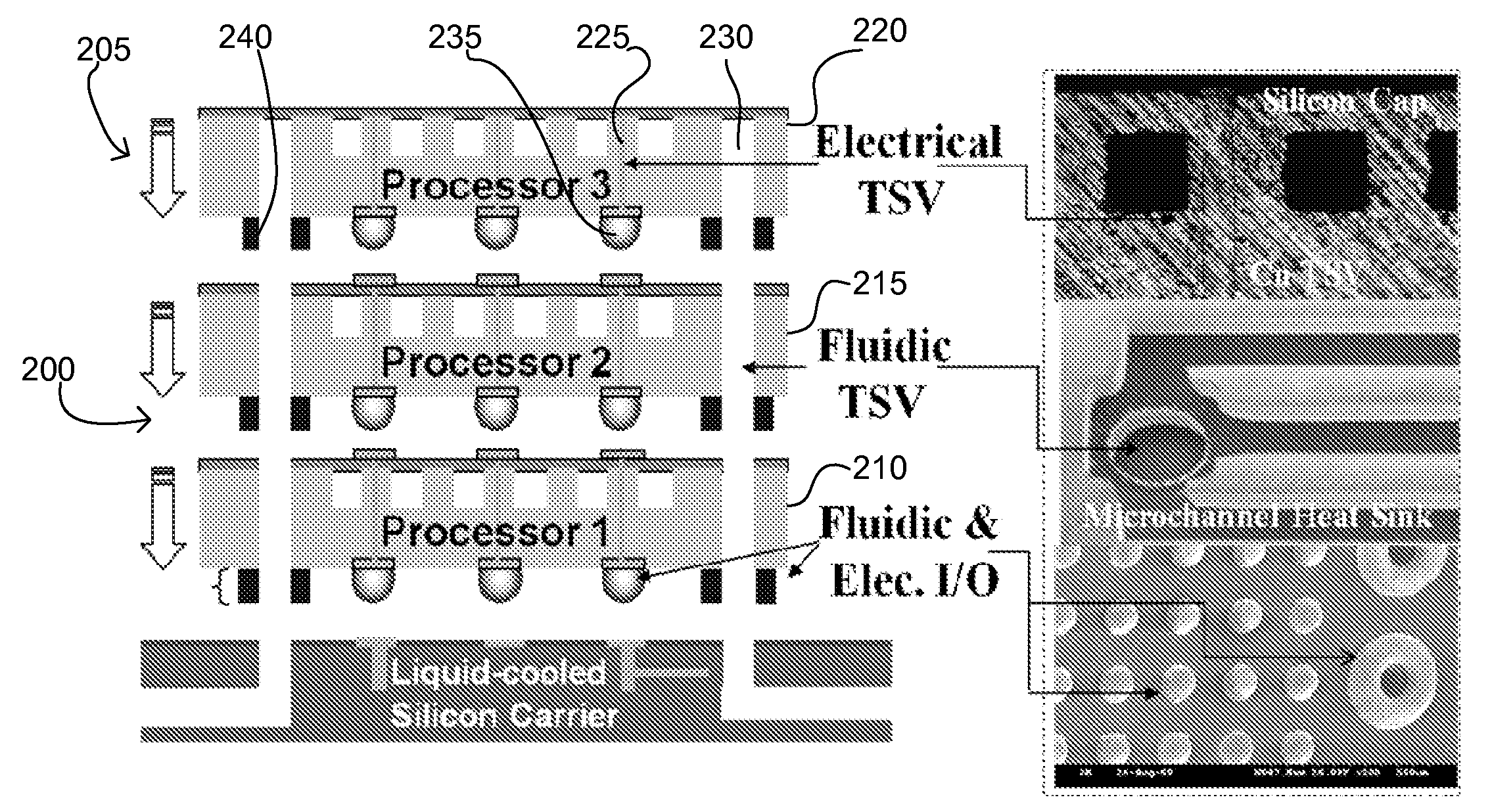
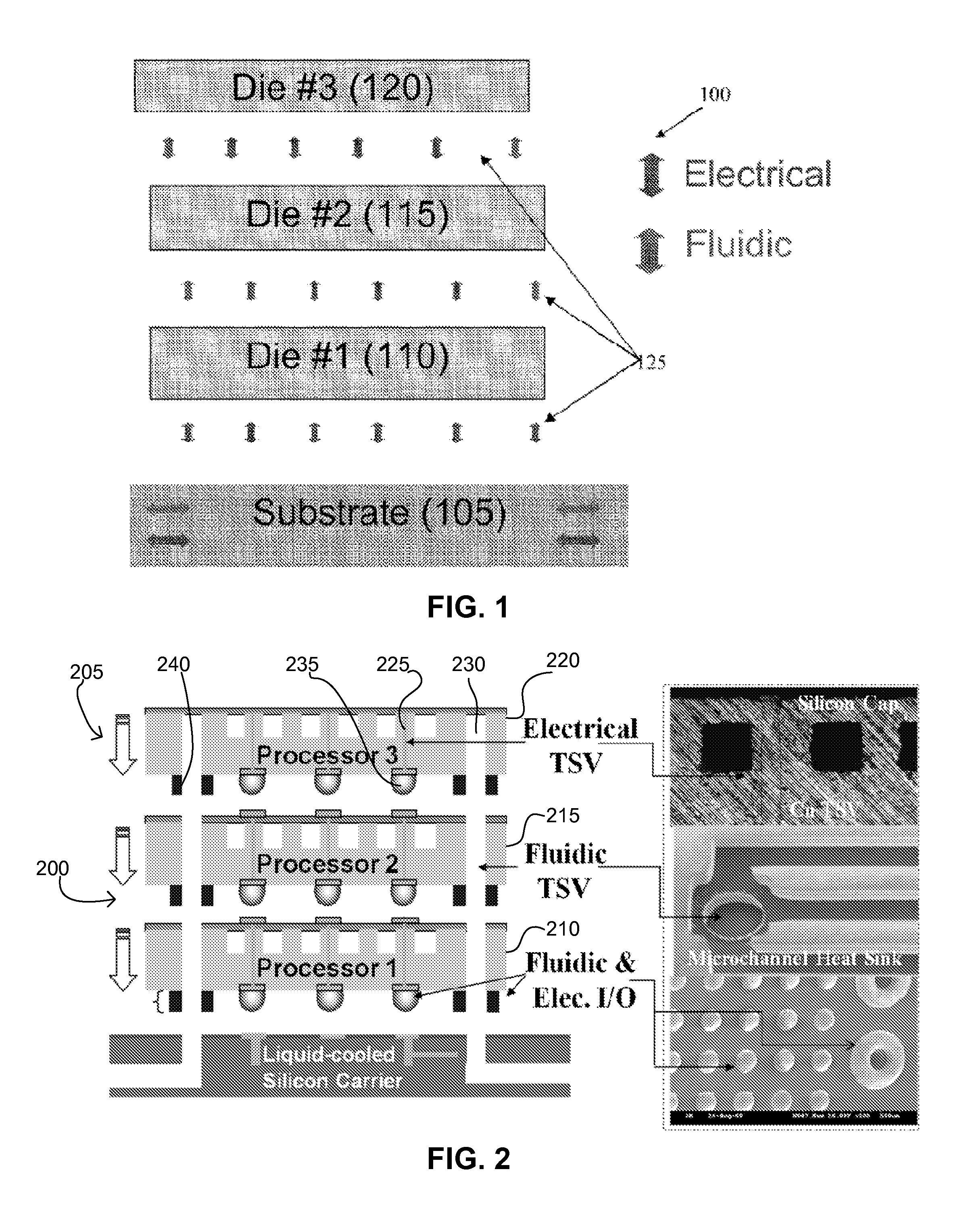
[0032]To facilitate an understanding of the principles and features of the present invention, various illustrative embodiments are explained below. In particular, the invention is described in the context of being 3D ICs and methods of fabricating the same.
[0033]The components described hereinafter as making up various elements of the invention are intended to be illustrative and not restrictive. Many suitable components or steps that would perform the same or similar functions as the components or steps described herein are intended to be embraced within the scope of the invention. Such other components or steps not described herein can include, but are not limited to, for example, similar components or steps that are developed after development of the invention.
[0034]Referring now to the figures, wherein like reference numerals represent like parts throughout the several views, exemplary embodiments of the present invention will be described in detail. Throughout this description,...
PUM
 Abstract
Description
Claims
Application Information