

Etching Gas
Inactive Publication Date: 2012-09-13
CENT GLASS CO LTD
View PDF5 Cites 10 Cited by
- Summary
- Abstract
- Description
- Claims
- Application Information
AI Technical Summary
Benefits of technology
[0016]In view of the above, an object of the present invention is to provide a novel etching gas which is not only excellent in etching performances but also easily available and does not substantially by-produce CF4 that places a burden on the environment.
Problems solved by technology
However, it is considered difficult to fundamentally avoid a recombination of the CF3 active species and the fluorine active species so long as the etching gas partially having the structure of CF3 group is used.
In view of the above, the optimized etching condition is found not to be optimized in respect of the micro-patterning speed and the patterning accuracy, which means that the aimed patterning accuracy and the like are restricted by the rate of CF4 by-production.
As the carbon number gets increased, F / C thus approaches 1 or the above-mentioned requirement, but the boiling point also gets increased so as to become difficult to handle as gas.
Method used
View moreImage
Smart ImageViewing Examples

Examples
examples
[0052]The present invention will be more readily understood with reference to the following Examples.
Login to View More PUM
| Property | Measurement | Unit |
|---|---|---|
| Fraction | aaaaa | aaaaa |
| Fraction | aaaaa | aaaaa |
| Time | aaaaa | aaaaa |
Abstract
Disclosed is an etching gas provided containing CHF2COF. The etching gas may contain, as an additive, at least one kind of gas selected from O2, O3, CO, CO2, F2, NF3, Cl2, Br2, I2, XFn (In this formula, X represents Cl, I or Br. n represents an integer satisfying 1≦n≦7.), CH4, CH3F, CH2F2, CHF3, N2, He, Ar, Ne, Kr and the like, from CH4, C2H2,C2H4,C2H6, C3H4, C3H6, C3H5, HI, HBr, HCl, CO, NO, NH3, H2 and the like, or from CH4, CH3F, CH2F2 and CHF3. This etching gas is not only excellent in etching performances such as the selection ratio to a resist and the patterning profile but also easily available and does not substantially by-produce CF4 that places a burden on the environment.
Description
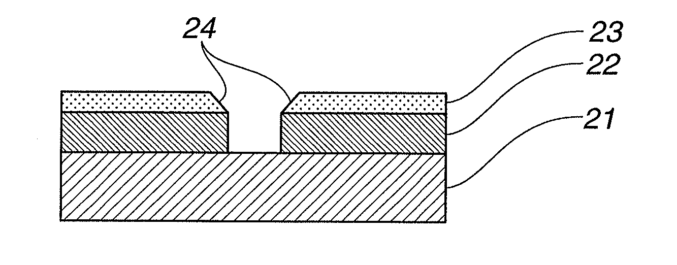
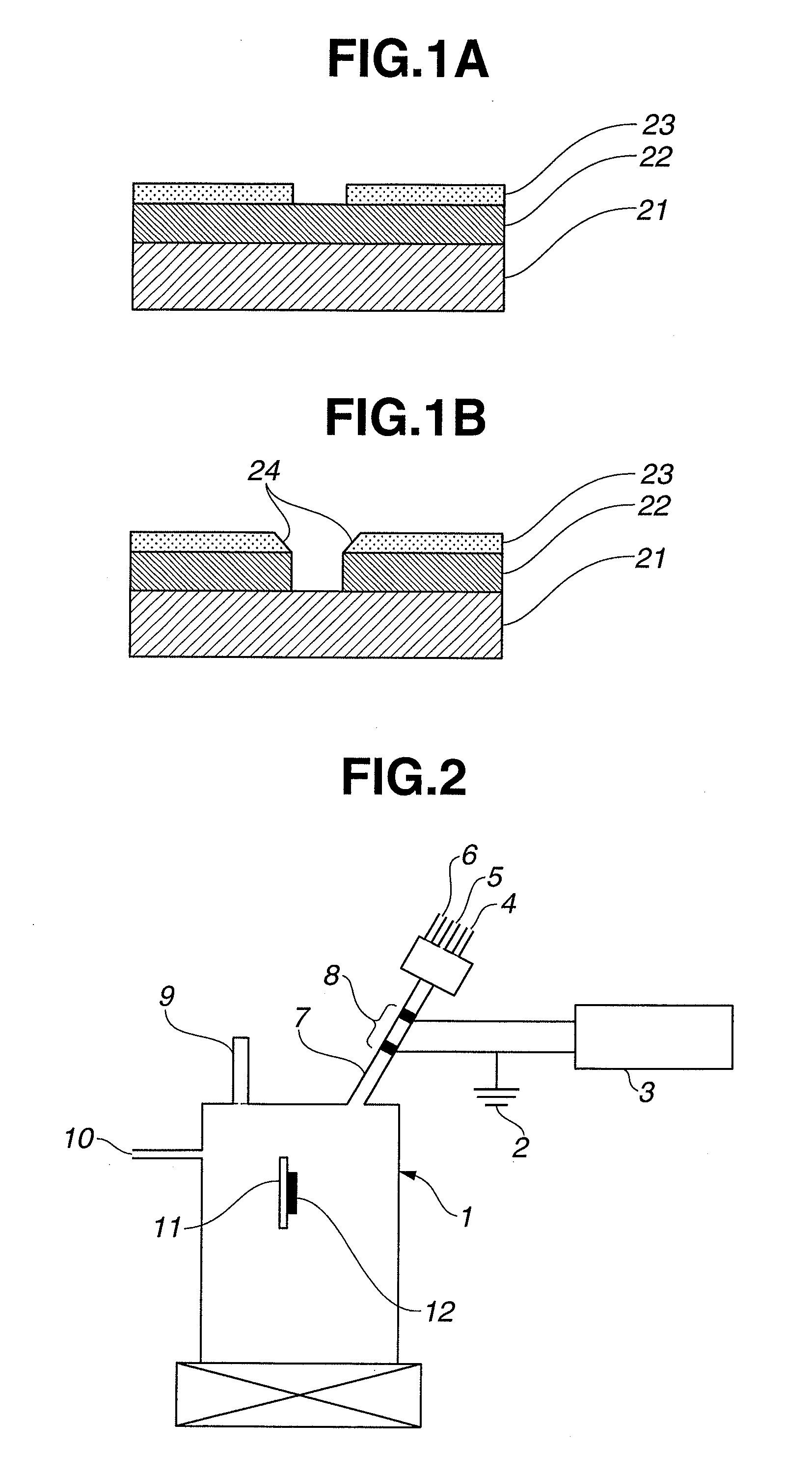
TECHNICAL FIELD[0001]The present invention relates to an etching gas used for producing thin film devices represented by IC, LSI, TFT and the like, and particularly to an etching gas that accomplishes both environmental performances and micro-patterning performances.BACKGROUND OF THE INVENTION[0002]In processes for producing semiconductor thin film devices, optical devices, super steel materials and the like, there have been produced various thin films, thick films and the like by means of CVD method, sputtering method, sol-gel method, vapor deposition method and the like. Moreover, in order to form a circuit pattern, gas etching for partially removing a thin film material has been conducted on semiconductors or in fabrication of semiconductors for IC, LSI, TFT and the like.[0003]Hitherto, perfluorocarbons (PFCs) such as CF4, C2F6, C3F8 and the like have been used as an etching gas in etching for forming circuits, in fabrication of thin film devices. However, these gases exist in th...
Claims
Login to View More Application Information
Patent Timeline
 IPC IPC(8): C09K13/00C09K13/06C07C49/88H01L21/306
CPCH01L21/3065C07C53/48C23F1/12C09K13/00H01L21/31116C07C19/08H01L21/0274
InventorTAKADA, NAOTOMORI, ISAMU
OwnerCENT GLASS CO LTD