Transistor circuit with protecting function

a technology of transistor circuit and protection function, applied in the direction of emergency protective circuit arrangement for limiting excess voltage/current, emergency protective circuit arrangement, etc., can solve the problem that controllers without mosfet protection function cannot ensure the mosfet is protected, the reliability of the mosfet may be decreased, and even damaged, etc. problems, to achieve the effect of lowering the cost and increasing the yield ra

Inactive Publication Date: 2012-09-20
GREEN SOLUTION TECH CO LTD
View PDF7 Cites 31 Cited by
  • Summary
  • Abstract
  • Description
  • Claims
  • Application Information

AI Technical Summary

Benefits of technology

[0006]The present invention provides a transistor circuit which has a MOSFET and a protecting circuit packaged in the same package to make sure that electric characteristics of semiconductor element(s) in the circuit to be equivalent. Therefore, the

Problems solved by technology

The reliability of the MOSFET may be decreased, even damaged, when the MOSFET is operated out of safe operating area.
However, not all MOSFET controllers detect the state of the MOSFET to protect it.
The controller without MOSFET protecting function cannot make sure that the MOSFET operates in the safe operating a

Method used


Image

  • Transistor circuit with protecting function
  • Transistor circuit with protecting function
  • Transistor circuit with protecting function

Examples


first embodiment

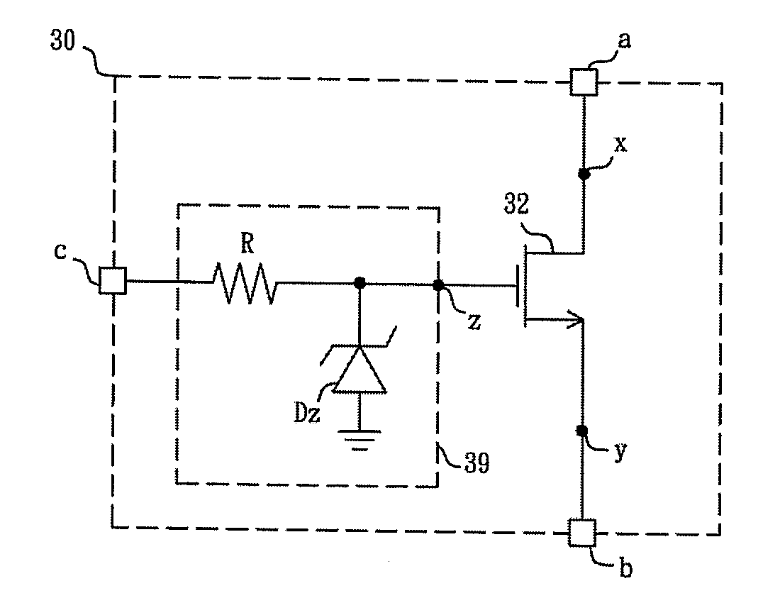
[0022]FIG. 2 is a schematic diagram of a transistor circuit with protecting function according to the present invention. A transistor circuit 30 is packaged in a single package structure having a first terminal a, a second terminal b, a control terminal c, and a protection terminal PROT, wherein the transistor circuit 30 comprises a transistor 32, a voltage detecting unit 34, a temperature detecting unit 38 and a protecting unit 200. The transistor 32 comprises a drain end x coupled to the first terminal a, a source end y coupled to the second terminal b, and a gate end z coupled to the control terminal c. In the present embodiment, take that a voltage drop between the drain end x and the source end y of the transistor 32 and a temperature of the transistor circuit 30 is too high for example, the circuit operations are described in the following. The voltage detecting unit 34 which detects the voltage drop of the transistor 32 comprises a voltage dividing element 34a and a comparato...

third embodiment

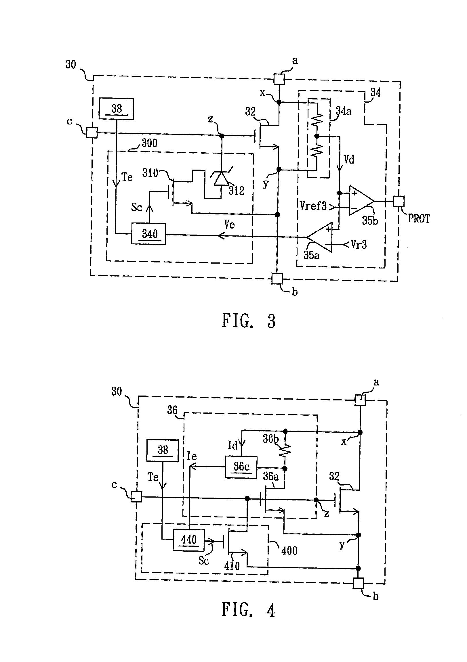
[0026]FIG. 4 is a schematic diagram of a transistor circuit with protecting function according to the present invention. A transistor circuit 30 is packaged in a single package structure having a first terminal a, a second terminal b and a control terminal c. The transistor 30 comprises a transistor 32, a current detecting unit 36, a temperature detecting unit 38 and a protecting unit 400. The transistor 32 comprises a drain end x coupled to the first terminal a, a source end y coupled to the second terminal b and a gate end z coupled to the control terminal c. The current detecting unit 36 is coupled to the first terminal a to detect the current flowing through the transistor 32. The current detecting unit 36 comprises a detecting transistor 36a, a current detecting resistance 36b and a current sensing element 36c. A drain end of the detecting transistor 36a is coupled to the drain end x of the transistor 32 through the current detecting resistance 36b, a source end thereof is coup...

fourth embodiment

[0030]FIG. 6 is a schematic diagram of a transistor circuit with protecting function applied to an LED driving circuit according to the present invention. The LED driving circuit comprises a power source supply unit 10, an LED module 20, a transistor circuit 30, a current detecting resistance 40 and an external control unit 50. The power source supply unit 10 is coupled to one terminal of the LED module 20 to supply a driving voltage VDD to drive the LED module 20 lighting. The transistor circuit 30 is packaged in a single package structure and coupled to another terminal of the LED module 20 to control an amount of a current flowing through the LED module 20 according to the a current control signal ISc. The current detecting resistance 40 is coupled to the transistor circuit 30 to detect the amount of the current flowing through the LED module 20 and generate a current feedback signal Ifb. The transistor circuit 30 comprises a transistor 32, a voltage detecting unit 34, a temperat...


PUM


Abstract

The present invention provides a transistor circuit with protecting function. The transistor circuit includes a transistor, a voltage detecting unit, a current detecting unit, a temperature detecting unit, and a protecting unit. The voltage detecting unit detects a voltage drop of the transistor and generates an over-voltage protection signal. The current detecting signal detects a current flowing through the transistor and generates an over-current protection signal. The temperature detecting unit detects a temperature of the transistor circuit and generates an over-temperature protection signal. The protecting unit is coupled to the control terminal to control a state of the transistor according to the over-voltage protection signal, the over-current protection signal, and the over-temperature protection signal to reduce the voltage difference between the control terminal and the second terminal, such that the voltage drop of the transistor is decreased or decreased to zero.

Description

BACKGROUND[0001]1. Field of the Invention[0002]The present invention relates to a transistor circuit with protecting function, and more particularly a transistor circuit with protecting function packaged in a single package.[0003]2. Description of Related Art[0004]A conventional MOSFET has a safe operating area (SOA) and the safe operating area is determined by a largest current, a largest power, a largest voltage and a largest temperature that the MOSFET is able to handle without damage. The reliability of the MOSFET may be decreased, even damaged, when the MOSFET is operated out of safe operating area. In conventional arts, a protecting circuit is connected to the MOSFET externally. The protecting circuit detects a state of the MOSFET (such as a current flowing through the MOSFET), judges whether the MOSFET operates in the safe operating area and protects the MOSFET from being damaged.[0005]However, not all MOSFET controllers detect the state of the MOSFET to protect it. The contr...

Claims


Application Information

Patent Timeline
IPC IPC(8): H02H3/20H02H5/04H02H3/08
CPCH03K17/0822Y02B20/341H05B33/0887H05B45/50H05B47/28H05B47/25H05B47/24Y02B20/30
Inventor YU, CHUNG-CHE
Owner GREEN SOLUTION TECH CO LTD
Why Eureka
Try Eureka