Light emitting device package and manufacturing method thereof

a technology of light emitting devices and led packaging, which is applied in the manufacture of printed circuits, electrical equipment construction details, lighting and heating apparatus, etc., can solve the problems of low marketability, low heat radiation efficiency of lead frame type led packages, and complicated led manufacturing, etc., and achieve the effect of efficient radiation of heat generated

Inactive Publication Date: 2012-09-20
SAMSUNG ELECTRONICS CO LTD
View PDF8 Cites 22 Cited by
  • Summary
  • Abstract
  • Description
  • Claims
  • Application Information

AI Technical Summary

Benefits of technology

[0009]According to an embodiment of the present invention, there may be provided a light emitting device (LED) package and a manufacturing method thereof, capable of efficiently radiating heat

Problems solved by technology

Heat radiation efficiency of the lead frame type LED package is relatively low since light is emitted through the lead frames.
In case

Method used


Image

  • Light emitting device package and manufacturing method thereof
  • Light emitting device package and manufacturing method thereof
  • Light emitting device package and manufacturing method thereof

Examples


Embodiment Construction

[0032]Reference will now be made in detail to exemplary embodiments of the present invention, examples of which are illustrated in the accompanying drawings, wherein like reference numerals refer to the like elements throughout. Exemplary embodiments are described below to explain the present invention by referring to the figures.

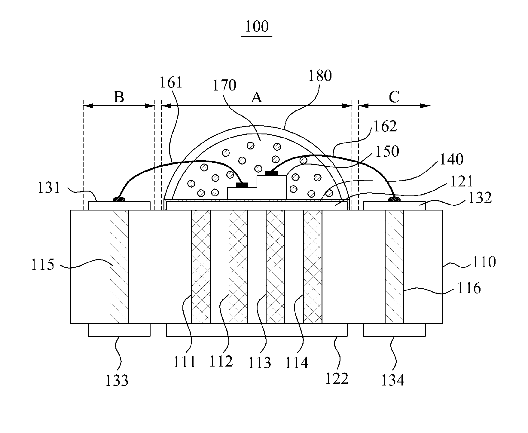
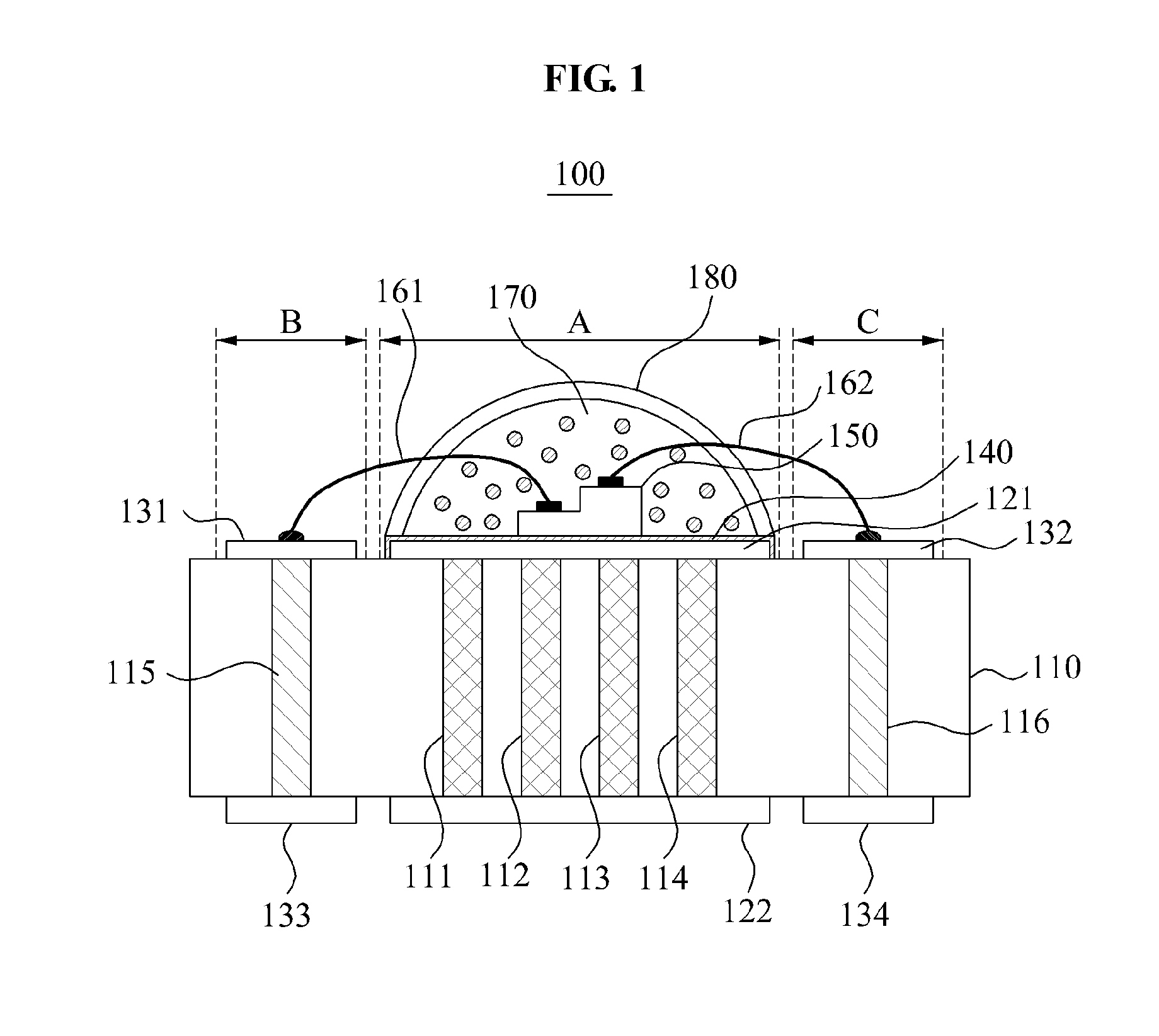
[0033]FIG. 1 illustrates a sectional view of a light emitting device (LED) package 100 according to an embodiment of the present invention. Referring to FIG. 1, the LED package 100 may include a circuit board 110, a first thermal pad 121, a second thermal pad 122, first electrode pads 131 and 132, second electrode pads 133 and 134, a reflection metal layer 140, an LED 150, a phosphor layer 170, and a molding portion 180.

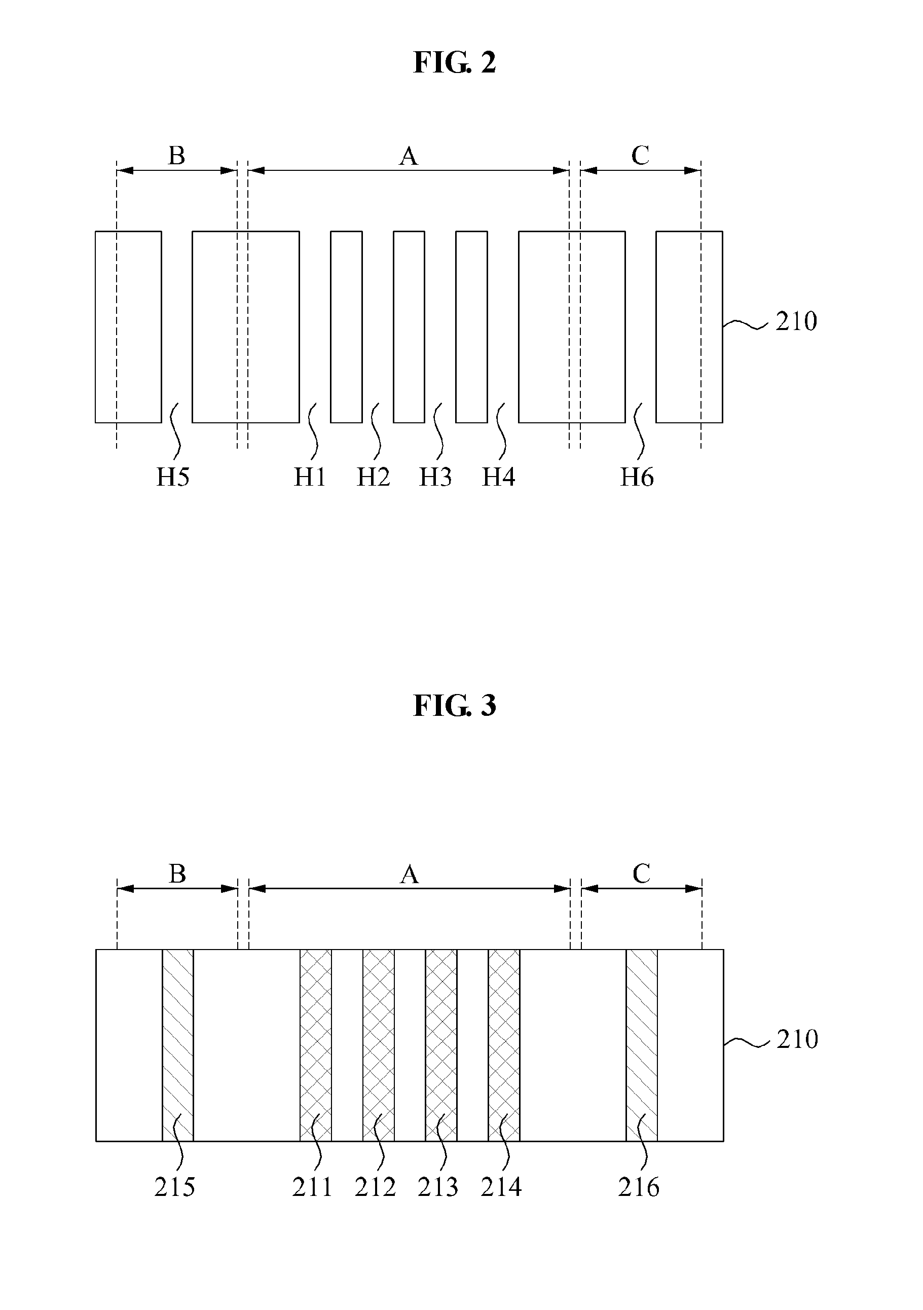
[0034]The circuit board 110 may be a metal core printed circuit board (PCB) or a Flame Resistant (FR) 4 substrate. The FR4 substrate may be a core-type substrate formed by coating a PCB, a ceramic substrate, or various other types of semicon...


PUM

PropertyMeasurementUnit
Timeaaaaaaaaaa
Thicknessaaaaaaaaaa
Thicknessaaaaaaaaaa

Abstract

A light emitting device (LED) package and a manufacturing method thereof are provided. The LED package includes a circuit board comprising at least one device region, a plurality of electrode regions, at least one first thermal via exposed through upper and lower surfaces of the at least one device region, and a plurality of second thermal vias exposed through upper and lower surfaces of the plurality of electrode regions; at least one first thermal pad bonded to the upper surface of the at least one device region and connected to the first thermal via; at least one LED mounted on the at least one first thermal pad; a plurality of first electrode pads bonded to the upper surface of the electrode region and connected to the second thermal vias; and a plurality of wires to connect the at least one LED with the plurality of first electrode pads.

Description

CROSS-REFERENCE TO RELATED APPLICATION[0001]This application claims the benefit of Korean Patent Application No. 10-2011-0022367, filed on Mar. 14, 2011, in the Korean Intellectual Property Office, the disclosure of which is incorporated herein by reference.BACKGROUND[0002]1. Field[0003]The present invention relates to a light emitting device (LED) package and a manufacturing method thereof, capable of achieving high performance efficiency and heat radiation efficiency.[0004]2. Description of the Related Art[0005]A light emitting device (LED) refers to a semiconductor device to convert electrical energy into optical energy. The LED consists of compound semiconductor materials that generate light of a particular wavelength according to an energy band gap. Use of the LED is expanding from optical communication, a display device such as a mobile display and a computer monitor, and a flat light source for a liquid crystal display (LCD), even to general lighting devices.[0006]In general,...

Claims


Application Information

Patent Timeline
IPC IPC(8): H05K7/20H05K3/30F21V29/00
CPCH01L33/60Y10T29/49139H01L33/647H01L33/642H01L2224/8592H01L2224/73265H01L2224/49107H01L2224/48227H01L2224/48091H01L2224/32225H01L2924/00014H01L2924/00H01L2924/181H01L2924/00012H01L33/20H01L33/62
Inventor LEE, DONG YEOULMIN, KYEONG IKLEE, CHANG SUB
Owner SAMSUNG ELECTRONICS CO LTD
Why Eureka
Try Eureka