Optical module

Active Publication Date: 2012-09-27
II VI DELAWARE INC +1
View PDF3 Cites 0 Cited by
  • Summary
  • Abstract
  • Description
  • Claims
  • Application Information

AI Technical Summary

Benefits of technology

[0006]An advantage of the present invention is that the carrier can be fabricated at very low cost. In contrast to semiconductor material, polymer material allows defining the carrier surface by moulding, only. As such, the entire carrier including all surface sections may be fabricated in a single moulding step, e. g. by injection moulding.
[0007]According to a preferred embodiment the optical module further comprises an amplifier arranged on a third surface section of the carrier and electrically connected to the converting element.
[0008]The amplifier and / or the converting element may be thermally coupled to a heat sink layer arranged on the second surface section and / or the third surface section of the carrier. This heat sink layer may extend into the first surface section and form the mirror, which then emits thermal energy generated by the amplifier and / or the converting element over the mirror surface.
[0009]The heat sink layer may also be electrically conductive. This allows electrically connecting the heat sink layer to at least one of the amplifier and the converter. E. g., the heat sink layer may form an electrically conducting ground of the optical module.
[0010]The heat sink layer may consist of or comprise metal since metal provides both, good thermal and electrical conductivity.
[0011]Further, a heat coupling section of the heat sink layer may be arranged between the carrier surface and the amplifier in order to provide a sufficient transfer of heat from the amplifier to the mirror surface. Alternatively or additionally, a heat coupling section of the heat sink layer may be arranged between the carrier surface and the converting element in order to provide a sufficient transfer of heat from the converter to the mirror surface.

Problems solved by technology

Devices like those described in the cited German Patent require costly fabrication processes as the carrier is made of semiconductor material.

Method used


Image

  • Optical module
  • Optical module
  • Optical module

Examples


Embodiment Construction

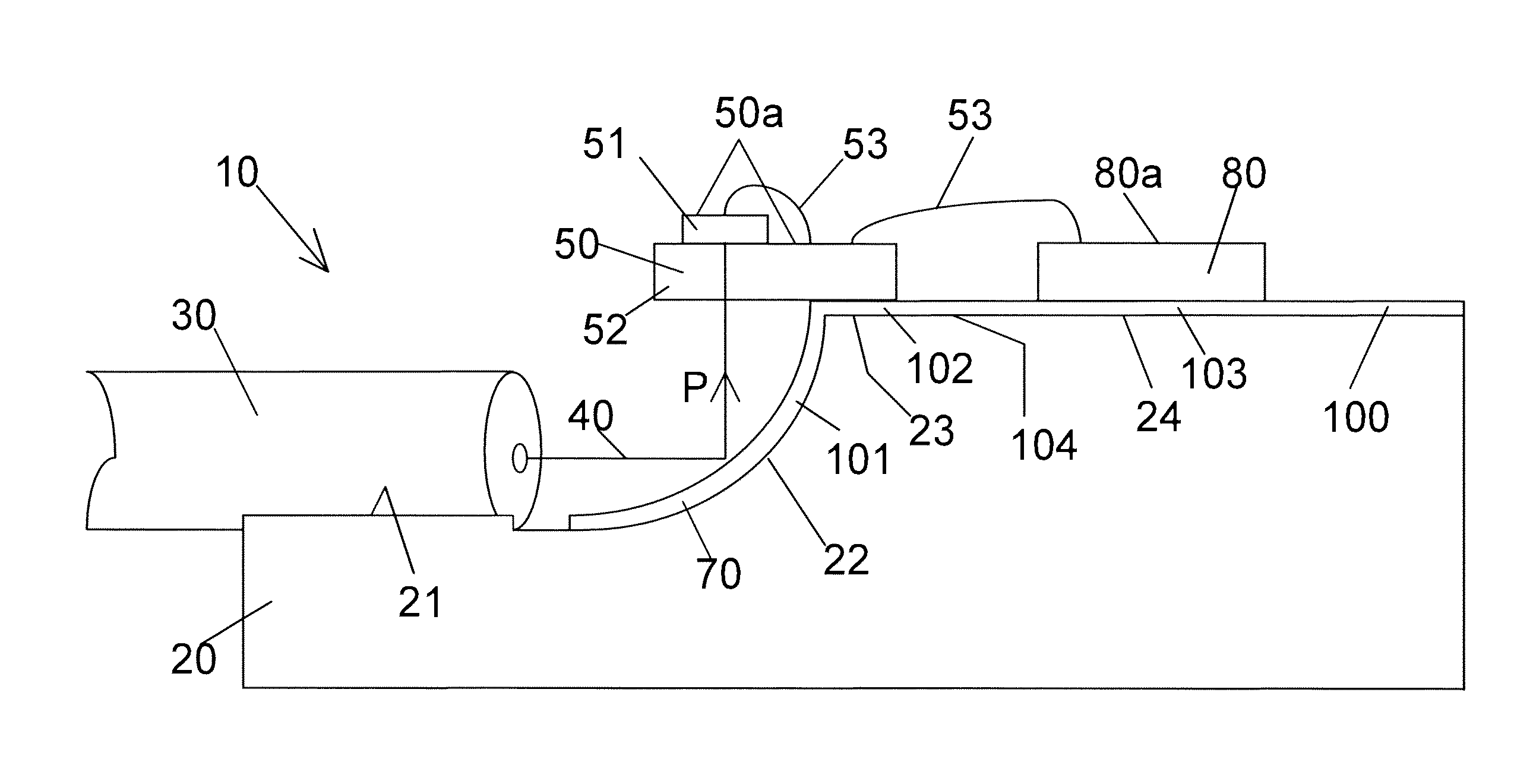
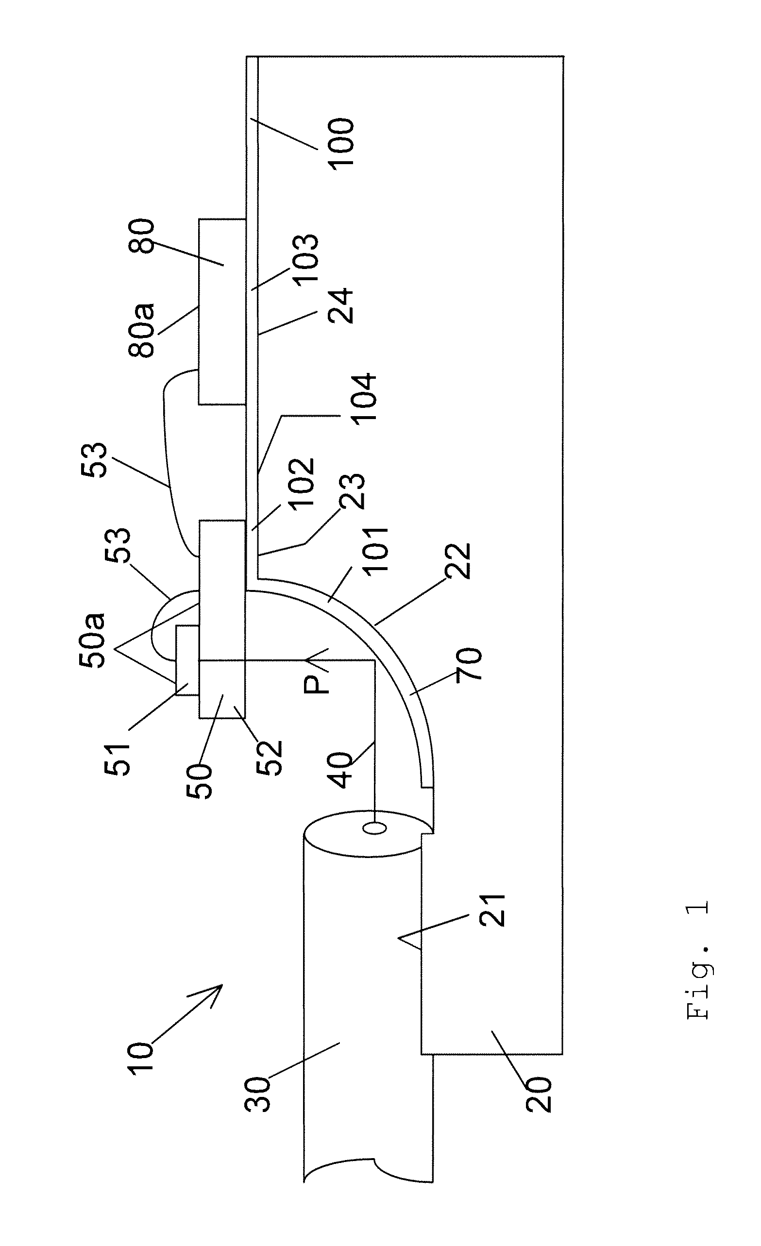
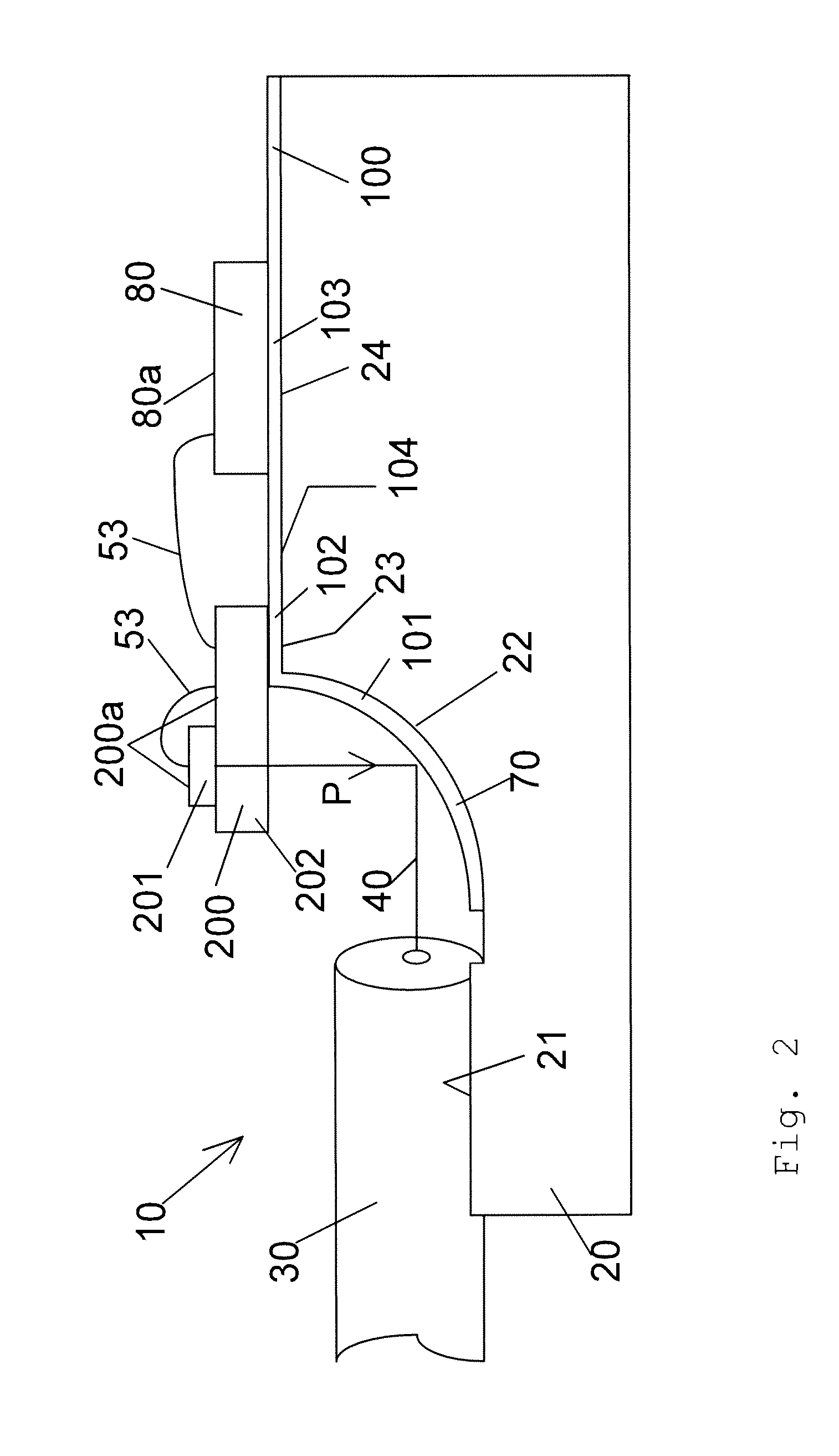
[0036]The preferred embodiment of the present invention will be best understood by reference to the drawings, wherein identical or comparable parts are designated by the same reference signs throughout.

[0037]It will be readily understood that the present invention, as generally described and illustrated in the figures herein, could vary in a wide range. Thus, the following more detailed description of the exemplary embodiments of the present invention, as represented in FIGS. 1-4, is not intended to limit the scope of the invention, as claimed, but is merely representative of presently preferred embodiments of the invention.

[0038]FIG. 1 shows a first exemplary embodiment of an optical module 10 according to the present invention. The optical module 10 comprises a carrier 20 which consists of polymer material. Preferably, the polymer carrier 20 is formed by an injection moulding process.

[0039]The optical module 10 further comprises a guiding element 30 adapted to guide optical radiat...


PUM


Abstract

The invention relates to an optical module 10) comprising a guiding element (30) adapted to guide optical radiation (P); a converting element (50, 200) adapted to convert received electrical energy into optical radiation or to convert received optical radiation into electrical energy; a mirror (70) arranged in the beam path (40) between the optical guiding element and the converting element and configured to optically connect the guiding element and the converting element; and a carrier (20) having a first surface section (22) for carrying the mirror and a second surface (23) section for carrying the converting element. The carrier is made of polymer material.

Description

[0001]The invention relates to an optical module comprising a guiding element, a converting element, a mirror, and a carrier.BACKGROUND OF THE INVENTION[0002]German Patent DE 35 43 558 C2 discloses an optical module comprising the features of the preamble of claim 1. In this module, the light arriving in an optical fibre is coupled to a photodetector, which is expediently connected to an amplifier immediately downstream. The optical fibre and photodetector are coupled via an optical deflecting element and mounted on a carrier element, which consists of single crystal semiconductor material such as silicon.[0003]Devices like those described in the cited German Patent require costly fabrication processes as the carrier is made of semiconductor material.OBJECTIVE OF THE PRESENT INVENTION[0004]An objective of the present invention is to provide an optical module which can be fabricated at lower costs than prior art devices but shows a competitive performance.BRIEF SUMMARY OF THE INVENTI...

Claims


Application Information

Patent Timeline
IPC IPC(8): G01J1/04H03F3/08
CPCG02B6/4214G02B6/4274G02B6/4272G02B6/4269
Inventor UNTERBORSCH, GUNTERJACOB, ALEXANDERBELING, ANDREAS
Owner II VI DELAWARE INC
Why Eureka
Try Eureka