System and Method for Increasing Productivity of Organic Light Emitting Diode Material Screening

a technology of organic light-emitting diodes and screening systems, applied in the direction of electrical equipment, basic electric elements, test/measurement of semiconductor/solid-state devices, etc., can solve the disadvantage of uniform processing across an entire substrate, the cost of obtaining such data is higher, and the time required to accumulate a wide variety of data is longer

Active Publication Date: 2012-09-27
INTERMOLECULAR
View PDF0 Cites 18 Cited by
  • Summary
  • Abstract
  • Description
  • Claims
  • Application Information

AI Technical Summary

Problems solved by technology

However, uniform processing across an entire substrate can be disadvantageous when optimizing, qualifying, or investigating new materials, new processes, and / or new process sequence integration schemes, since the entire substrate is nominally made the same using the same materials, processes, and process sequence integration scheme.
Thus, the full substrate uniform processing under conventional processing techniques results in fewer data points per substrate, longer times to accumulate a wide variety of data, and higher costs associated with obtaining such data.
ITO, however, has several drawbacks, including a high manufacturing cost that, in turn, affects the price of devices based on OLED technology and thereby affects the ability of OLED-based devices to fully realize their potential in the marketplace.
The high manufacturing cost of ITO is attributed to, for example, the cost of indium, special equipment capable of accommodating the fragility of ITO, and the cost of deposition equipment, wherein ITO requires deposition in a vacuum.
Conventional research and development, however, is slow and costly.
For example, to know the result of each condition (e.g., as part of a design of experiments matrix), one wafer or coupon with many follow-up steps is required, which under current technology is very complicated as well as cost inefficient.
This approach has resulted in high R&D costs and the inability to conduct extensive experimentation in a timely and cost effective manner.

Method used


Image

  • System and Method for Increasing Productivity of Organic Light Emitting Diode Material Screening
  • System and Method for Increasing Productivity of Organic Light Emitting Diode Material Screening
  • System and Method for Increasing Productivity of Organic Light Emitting Diode Material Screening

Examples


Embodiment Construction

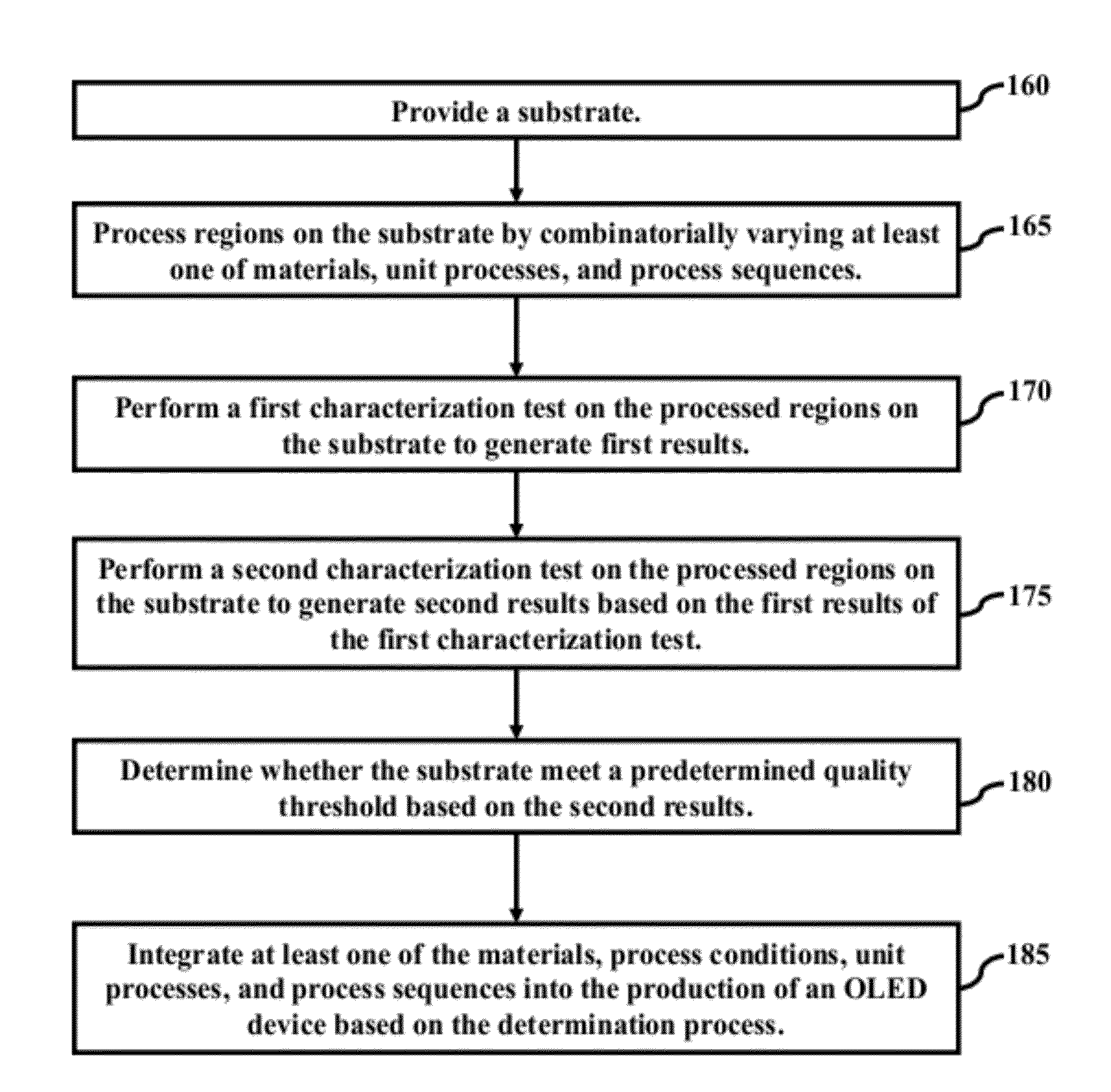
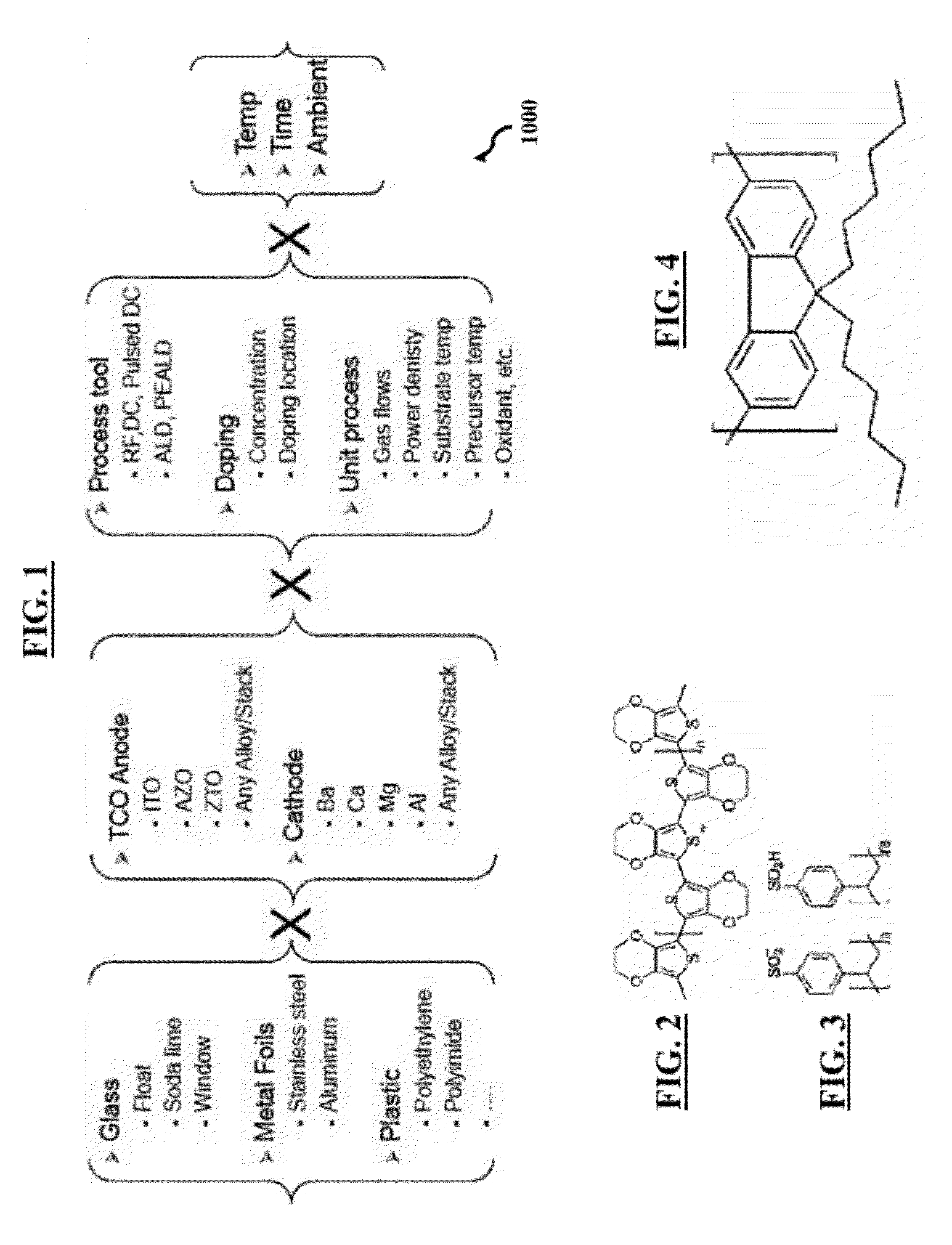
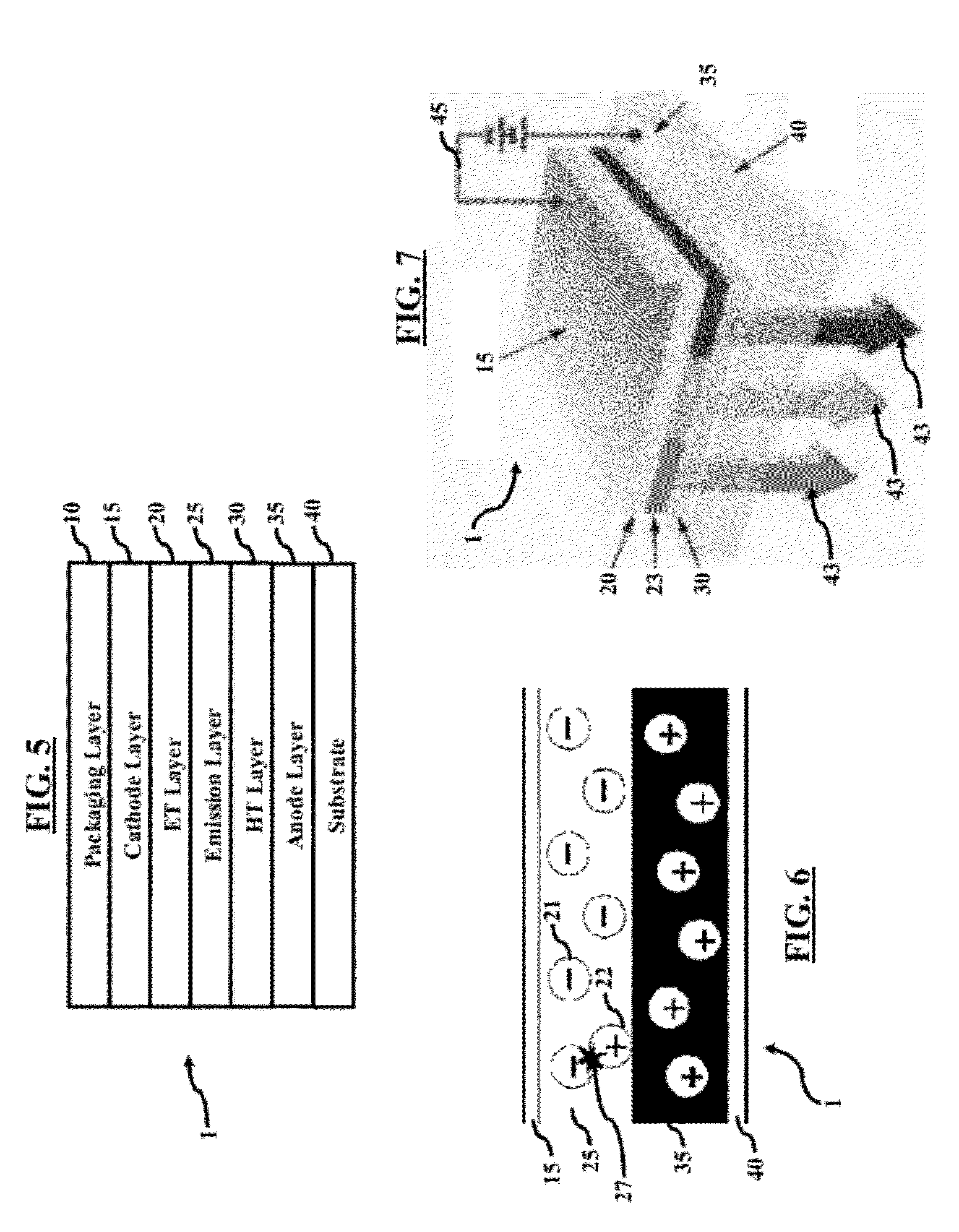
[0049]The embodiments herein and the various features and advantageous details thereof are explained more fully with reference to the non-limiting embodiments that are illustrated in the accompanying drawings and detailed in the following description. Descriptions of well-known components and processing techniques are omitted so as to not unnecessarily obscure the embodiments herein. The examples used herein are intended merely to facilitate an understanding of ways in which the embodiments herein may be practiced and to further enable those of skill in the art to practice the embodiments herein. Accordingly, the examples should not be construed as limiting the scope of the embodiments herein.

[0050]The embodiments herein provide a high performance combinatorial system and method that saves both operator resources as well as test time, and offers a key function for high throughput and combinatorial research. Referring now to the drawings, and more particularly to FIGS. 1 through 38, ...


PUM


Abstract

A system and method of increasing productivity of OLED material screening includes providing a substrate that includes an organic semiconductor, processing regions on the substrate by combinatorially varying parameters associated with the OLED device production on the substrate, performing a first characterization test on the processed regions on the substrate to generate first results, processing regions on the substrate in a combinatorial manner by varying parameters associated with the OLED device production on the substrate based on the first results of the first characterization test, performing a second characterization test on the processed regions on the substrate to generate second results, and determining whether the substrate meets a predetermined quality threshold based on the second results.

Description

BACKGROUND[0001]1. Technical Field[0002]The embodiments herein generally relate to organic light emitting diode processing and characterization, and more specifically, to a high throughput combinatorial screening through novel substrates and techniques.[0003]2. Description of the Related Art[0004]The ability to process uniformly across a monolithic substrate and / or across a series of monolithic substrates is advantageous for manufacturing efficiency and cost effectiveness, as well as repeatability and control. However, uniform processing across an entire substrate can be disadvantageous when optimizing, qualifying, or investigating new materials, new processes, and / or new process sequence integration schemes, since the entire substrate is nominally made the same using the same materials, processes, and process sequence integration scheme. In conventional processing systems, each processed substrate generally represents, in essence, only one possible variation per substrate. Thus, th...

Claims


Application Information

Patent Timeline
Patent Type & Authority Applications(United States)
IPC IPC(8): H01L21/66
CPCH01L51/56H01L51/0031H10K71/70H10K71/00
Inventor WANG, YUNCHIANG, TONY P.LANG, CHI-I
Owner INTERMOLECULAR
Why Eureka
Try Eureka