Semiconductor wafer and method of producing the same
- Summary
- Abstract
- Description
- Claims
- Application Information
AI Technical Summary
Benefits of technology
Problems solved by technology
Method used
Image

Examples
example 1
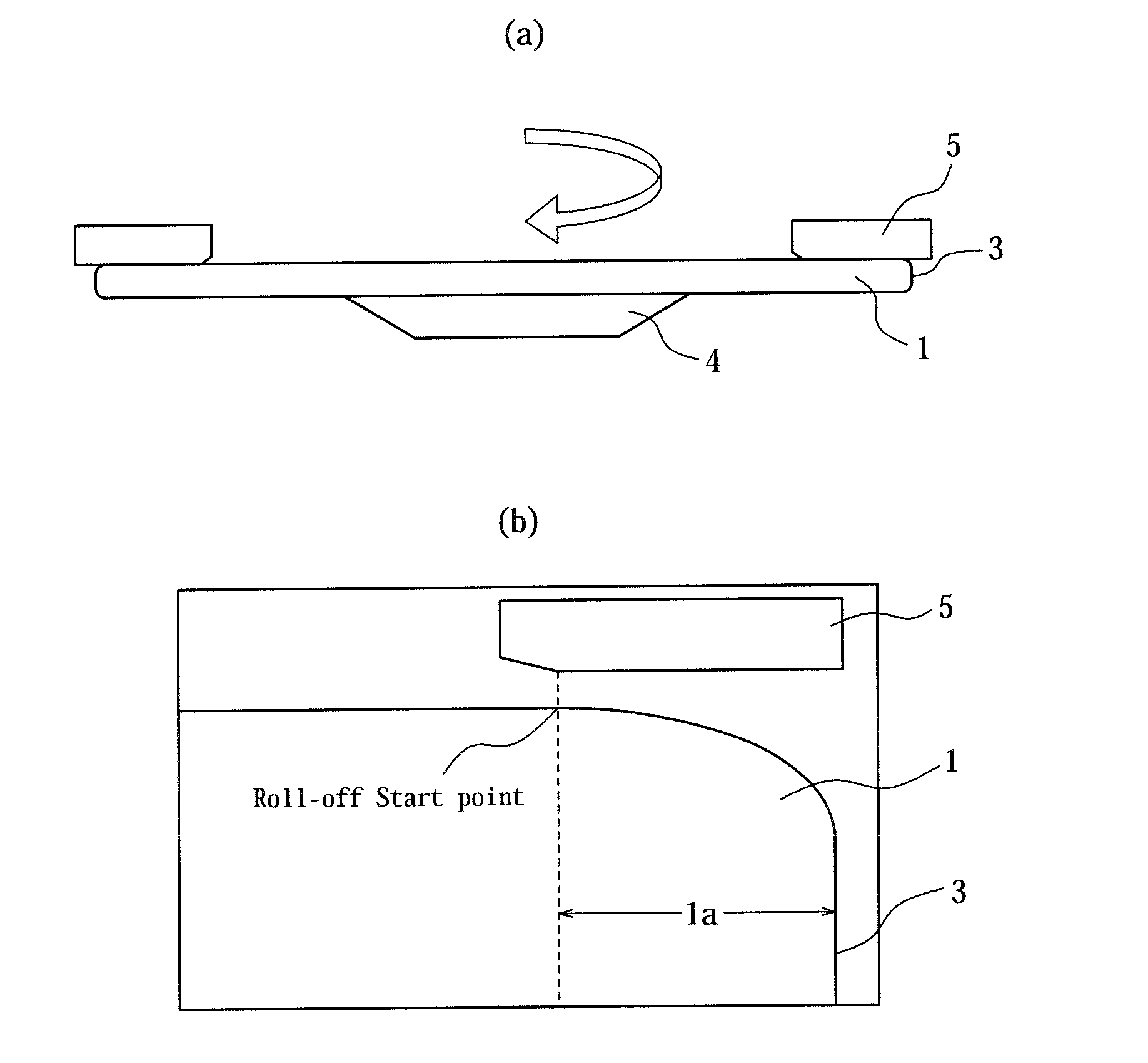
[0045]FIGS. 4(a) and 4(b) are diagrams illustrating a method of polishing an outer peripheral portion of a wafer in Example 1. FIG. 4(a) is a cross-sectional view schematically illustrating an apparatus for polishing an outer peripheral portion, and FIG. 4(b) is a cross-sectional view including a ring-shaped polishing cloth and an edge portion of a semiconductor wafer.
[0046]For polishing the outer peripheral portion of the semiconductor wafer 1, the apparatus in FIG. 4(a) includes a rotation stage 4 for holding the semiconductor wafer 1 and rotating it about the central axis, and a ring-shaped polishing cloth 5 for polishing only a region extending about 2 mm from the edge of the wafer 1. The ring-shaped polishing cloth 5 rotates in the direction opposite to the rotation direction of the wafer 1. Using the ring-shaped polishing cloth 5, the ring-shaped polishing cloth 5 can be uniformly pressed against the outer peripheral portion of the wafer, which prevents stress from being conce...
example 2
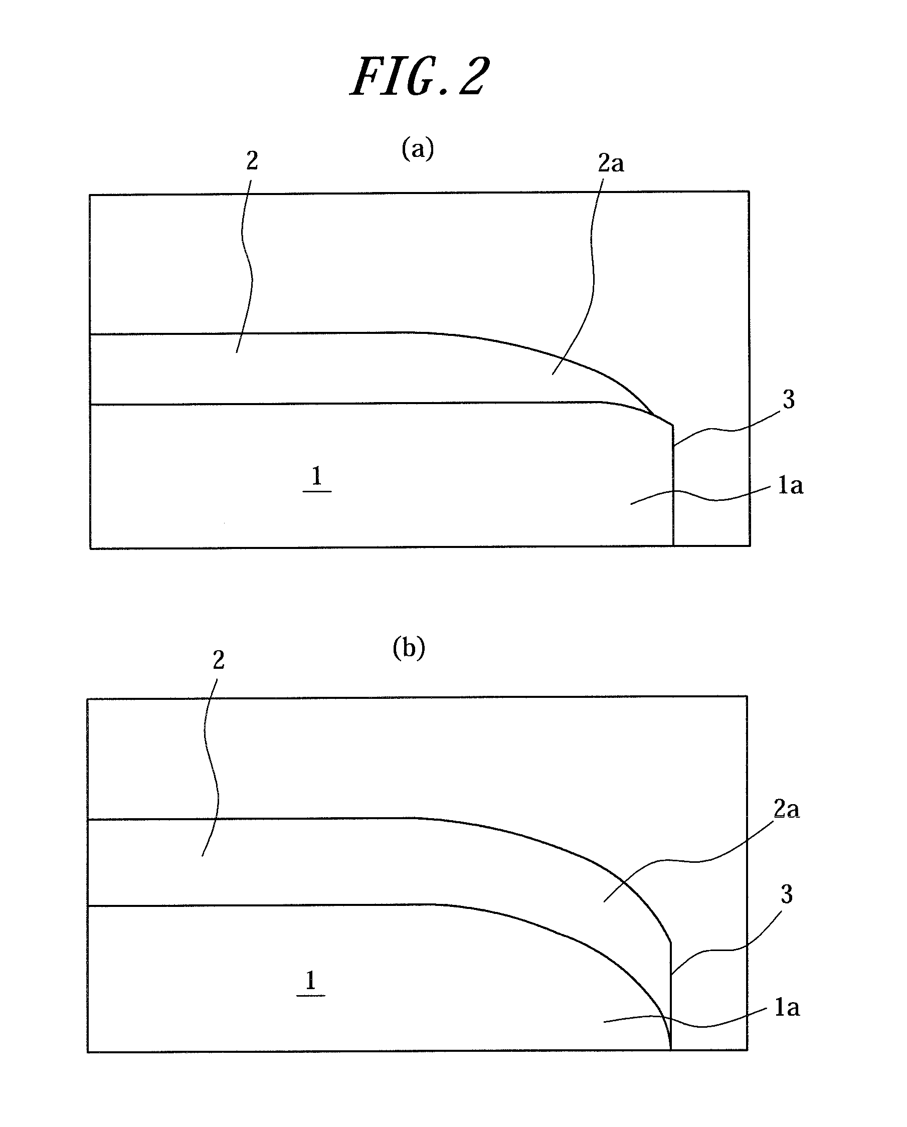
[0055]FIGS. 8(a) and 8(b) are diagrams illustrating a method of polishing an outer peripheral portion of a wafer 1 according to Example 2. FIG. 8(a) is a cross-sectional view schematically illustrating an apparatus for polishing an outer peripheral portion, and FIG. 8(b) is a cross-sectional view including a ring-shaped polishing cloth 5 and an edge portion of the semiconductor wafer 1. Example 2 is different from Example 1 in that a polishing cloth with which a region extending about 5 mm from the wafer edge can be polished was used as the ring-shaped polishing cloth 5, and the polishing time was 90 seconds which was longer than that in Example 1. The structure and the implementation steps other than the above are the same as Example 1, so the explanation will be omitted.
[0056]According to Example 2, the rolling off may start at a position about 5 mm distant from the edge of the semiconductor wafer 1 where the ring-shaped polishing cloth 5 contacts the semiconductor wafer 1 as show...
PUM
| Property | Measurement | Unit |
|---|---|---|
| Length | aaaaa | aaaaa |
| Length | aaaaa | aaaaa |
| Length | aaaaa | aaaaa |
Abstract
Description
Claims
Application Information
 - Generate Ideas
- Intellectual Property
- Life Sciences
- Materials
- Tech Scout
- Unparalleled Data Quality
- Higher Quality Content
- 60% Fewer Hallucinations
Browse by: Latest US Patents, China's latest patents, Technical Efficacy Thesaurus, Application Domain, Technology Topic, Popular Technical Reports.
© 2025 PatSnap. All rights reserved.Legal|Privacy policy|Modern Slavery Act Transparency Statement|Sitemap|About US| Contact US: help@patsnap.com