Optical modulator module and method for modulating optical signal

a technology of optical modulator and optical signal, which is applied in the direction of optics, instruments, electrical equipment, etc., can solve the problems of reducing the modulation bandwidth, and no practical optical modulator which can surpass

Active Publication Date: 2012-10-04
NEC CORP
View PDF1 Cites 71 Cited by
  • Summary
  • Abstract
  • Description
  • Claims
  • Application Information

AI Technical Summary

Benefits of technology

[0034]According to exemplary aspects of the present invention, it is possible to provide a compact, broad-band, and low-drive-voltage optical modulator module capable of generating any multilevel optical modulation signal simply by inputting a digital signal.

Problems solved by technology

However, since there is no practical optical modulator which surpasses the LN-based MZ optical intensity modulator in high-speed long distance optical transmission properties, it is still widely used for an optical transmitter unit or the like in various optical communication systems in trunk line networks.
Therefore, voltage distribution of the electrode is no longer regarded as uniform in an optical signal propagation axis direction.
As a result, this impedance mismatch leads to degradation of the modulation bandwidth due to reflection or the like and increase in driving voltage when the modulation electric signal output from the driving circuit is applied to the optical modulator as a transmission line.
This velocity mismatch between the modulated optical signal and the modulation electric signal limits the effective interaction length therebetween.
This leads to degradation of the modulation bandwidth and increase in driving current, as in the case of an impedance mismatch.
Thus, in the case of employing the traveling-wave type electrode is employed in the waveguide-type optical phase modulator or the electro absorption type optical intensity modulator, to which the p-i-n type diode structure is applied, there are problems in reduction in operation voltage and increase in bandwidth.

Method used


Image

  • Optical modulator module and method for modulating optical signal
  • Optical modulator module and method for modulating optical signal
  • Optical modulator module and method for modulating optical signal

Examples


first exemplary embodiment

[0049]Hereinafter, exemplary embodiments of the present invention will be described with reference to the drawings.

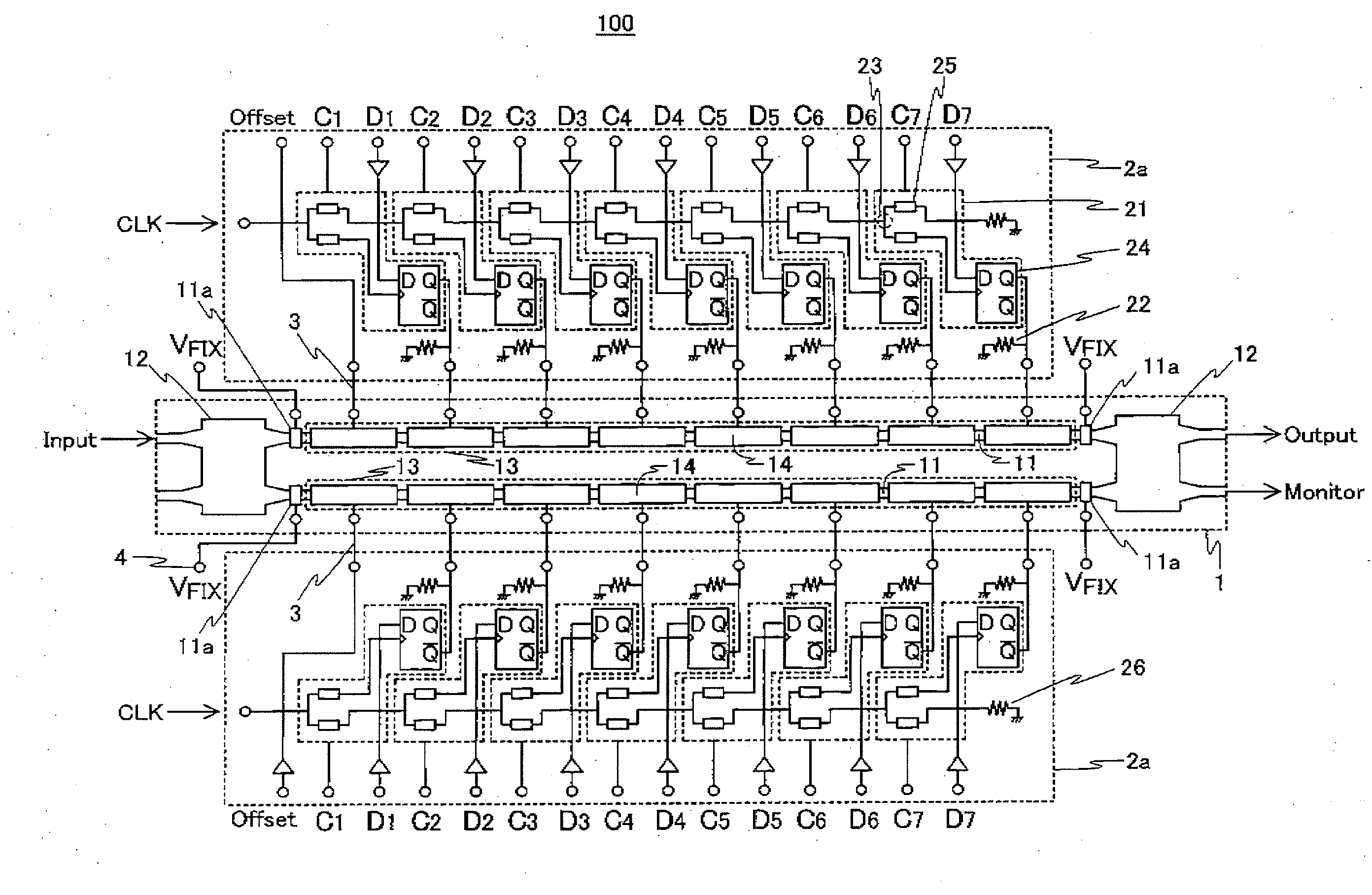
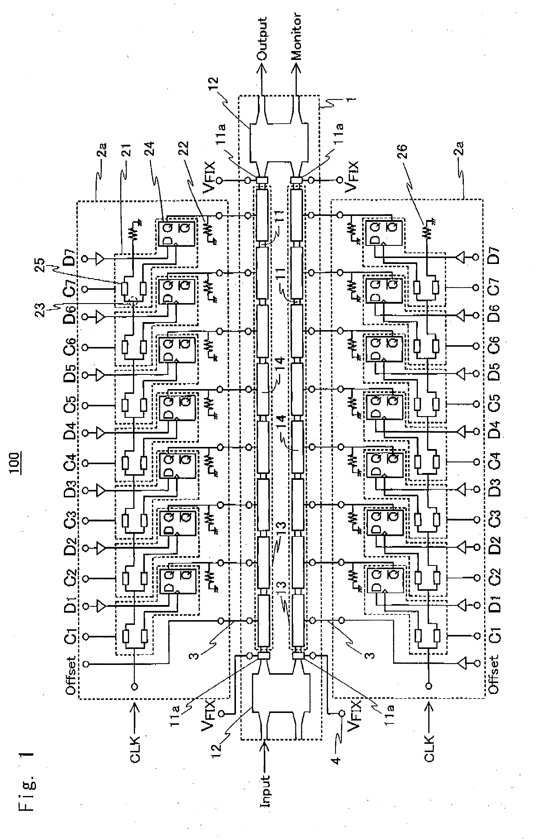
[0050]FIG. 1 is a block diagram of a digital segmented electrode structure multilevel optical modulator module 100, which is an exemplary digital segmented electrode structure multilevel optical modulator module, according to a first exemplary embodiment. The configuration of the digital segmented electrode structure multilevel optical modulator module 100 will be described below. As shown in FIG. 1, the digital segmented electrode structure multilevel optical modulator module 100 includes a digital segmented electrode structure optical modulator 1 and two integrated circuits 2a.

[0051]The digital segmented electrode structure optical modulator 1 has an MZ interferometer structure including two single-mode semiconductor optical waveguides 11 and a two-input / two-output optical multiplexer / demultiplexer 12. As shown in FIG. 1, optical signal Input is launched from the lef...

first example

[0077]A first example is an example of operation verification of the digital segmented electrode structure multilevel optical modulator module 100 according to the first exemplary embodiment.

[0078]In this example, the semiconductor optical waveguides 11 of the digital segmented electrode structure optical modulator 1 are formed on an Fe-doped-InP semi-insulating substrate (not shown). A core layer and cladding layers sandwiching the core layer are formed on the Fe-doped InP semi-insulating substrate. The core layer is formed of an undoped AlGaInAs multi-quantum well layer (the number of well layers: 12; well layer thickness: 10 nm; barrier layer thickness: 8 nm; transition wavelength: 1400 nm) and undoped InGaAsP light confining layers (wavelength composition: 1300 nm; thickness: 20 nm) formed on and under the undoped AlGaInAs multi-quantum well layer, and has a so-called separate confinement heterostructure (each of which is not shown). The cladding layers are made of p-type and n-...

second exemplary embodiment

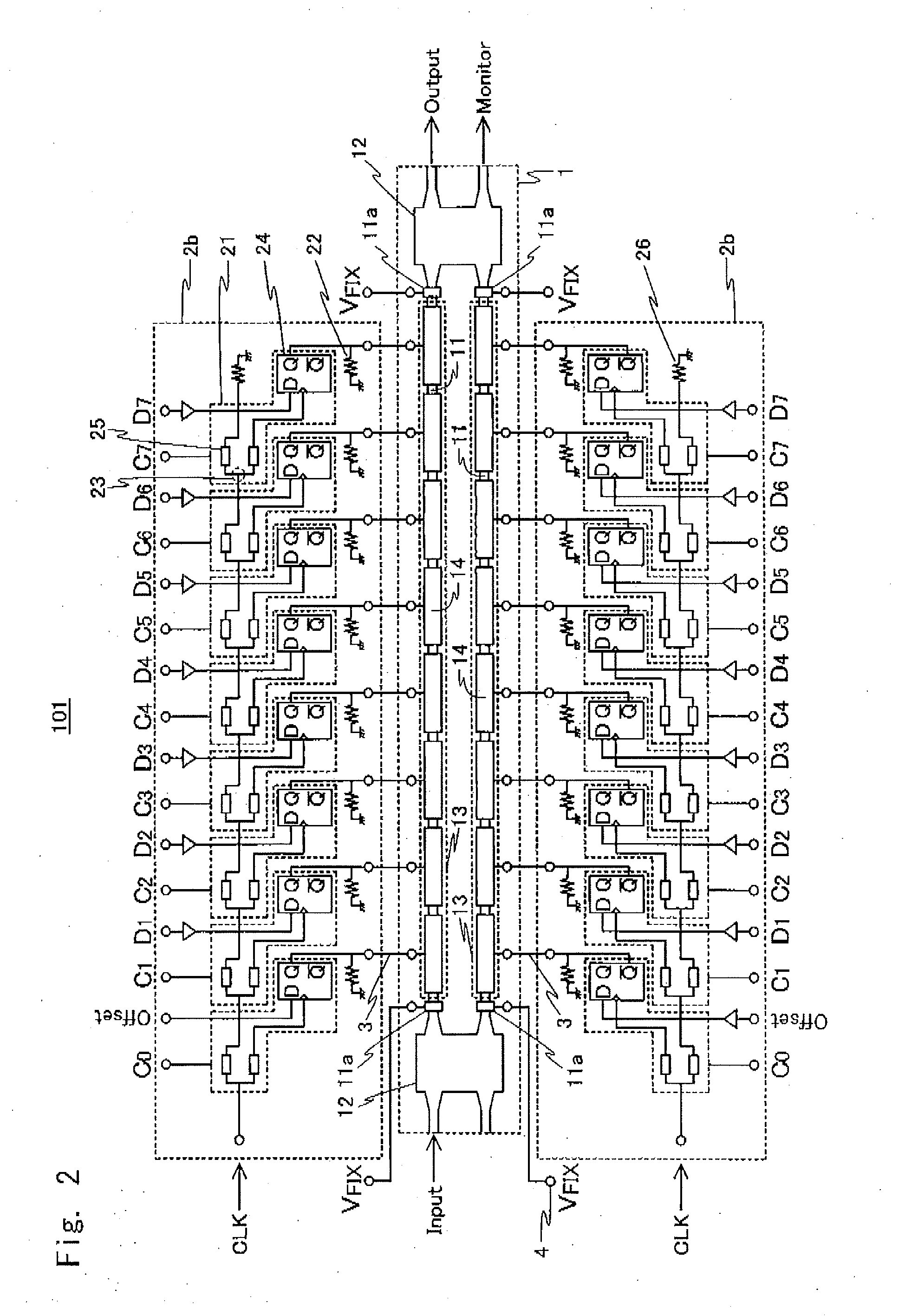
[0082]Next, a digital segmented electrode structure programmable multilevel optical modulator module 200 according to a second exemplary embodiment will be described. FIG. 3 is a block diagram of the digital segmented electrode structure programmable multilevel optical modulator module 200. As shown in FIG. 3, the digital segmented electrode structure programmable multilevel optical modulator module 200 has a configuration in which the integrated circuit 2a of the digital segmented electrode structure multilevel optical modulator module 100 is replaced with an integrated circuit 2c. In the integrated circuit 2c, an input interface for a digital input signal is changed so as to select 2(m-1) stages of waveguide-type optical phase modulator regions to be driven, unlike the integrated circuit 2a The D terminal of the individual driving circuit connected to the second-stage waveguide-type optical phase modulator region 14 receives the offset signal Offset, for example. The subsequent st...


PUM

PropertyMeasurementUnit
lengthaaaaaaaaaa
lengthaaaaaaaaaa
impedanceaaaaaaaaaa

Abstract

The present invention provides a compact, broad-band, and low-drive-voltage optical modulator module capable of generating any multilevel optical modulation. The optical modulator module according to an exemplary aspect of the present invention includes a digital segmented electrode structure optical modulator and m individual driving circuits. The digital segmented electrode structure optical modulator includes semiconductor optical waveguides and at least m waveguide-type optical phase modulator regions. An i-th individual driving circuit includes a driving circuit and a phase shift circuit. The driving circuit amplifies a digital input signal in synchronization with a clock signal and outputs the signal to an i-th waveguide-type optical phase modulator region. The phase shift circuit applies a delay to a signal branched from the clock signal. A j-th individual driving circuit receives an output signal from the phase shift circuit of a (j−1)-th individual driving circuit as a clock signal.

Description

[0001]This is a continuation of International Application PCT / JP2010 / 006012, with an international filing date of Oct. 7, 2010, which is hereby incorporated by reference herein its entirety.TECHNICAL FIELD[0002]The present invention relates to an optical modulator module and a method for modulating an optical signal. In particular, the present invention relates to a Mach-Zehnder type optical modulator module and a method for modulating an optical signal in a Mach-Zehnder type optical modulator module.BACKGROUND ART[0003]With an explosive increase in demand of a broadband multimedia communication service such as the Internet or a high-definition digital TV broadcast, a dense wavelength-division multiplexing optical fiber communication system, which is suitable for a long-distance and large-capacity transmission and is highly reliable, has been introduced in trunk line networks and metropolitan area networks. In access networks, an optical fiber access service spreads rapidly. In such...

Claims


Application Information

Patent Timeline
Patent Type & Authority Applications(United States)
IPC IPC(8): G02F1/035
CPCG02F1/0327G02F2201/127G02F2201/16H04B10/556
Inventor KATO, TOMOAKI
Owner NEC CORP
Why Eureka
Try Eureka