
Middle of line structures and methods for fabrication

Inactive Publication Date: 2012-10-18
ALSEPHINA INNOVATIONS INC
View PDF8 Cites 47 Cited by
  • Summary
  • Abstract
  • Description
  • Claims
  • Application Information

AI Technical Summary

Problems solved by technology

Without a nitride stop layer, it is extremely challenging for oxide etching processes to stop on the top of the gate or on the top of source / drain areas without damaging the silicide.
This shrinking of contact hole open area can cause severe aspect ratio dependent etching (ARDE) or the so called reactive ion etch (RIE) lag effect.

Method used


Image

  • Middle of line structures and methods for fabrication
  • Middle of line structures and methods for fabrication
  • Middle of line structures and methods for fabrication

Examples


Embodiment Construction

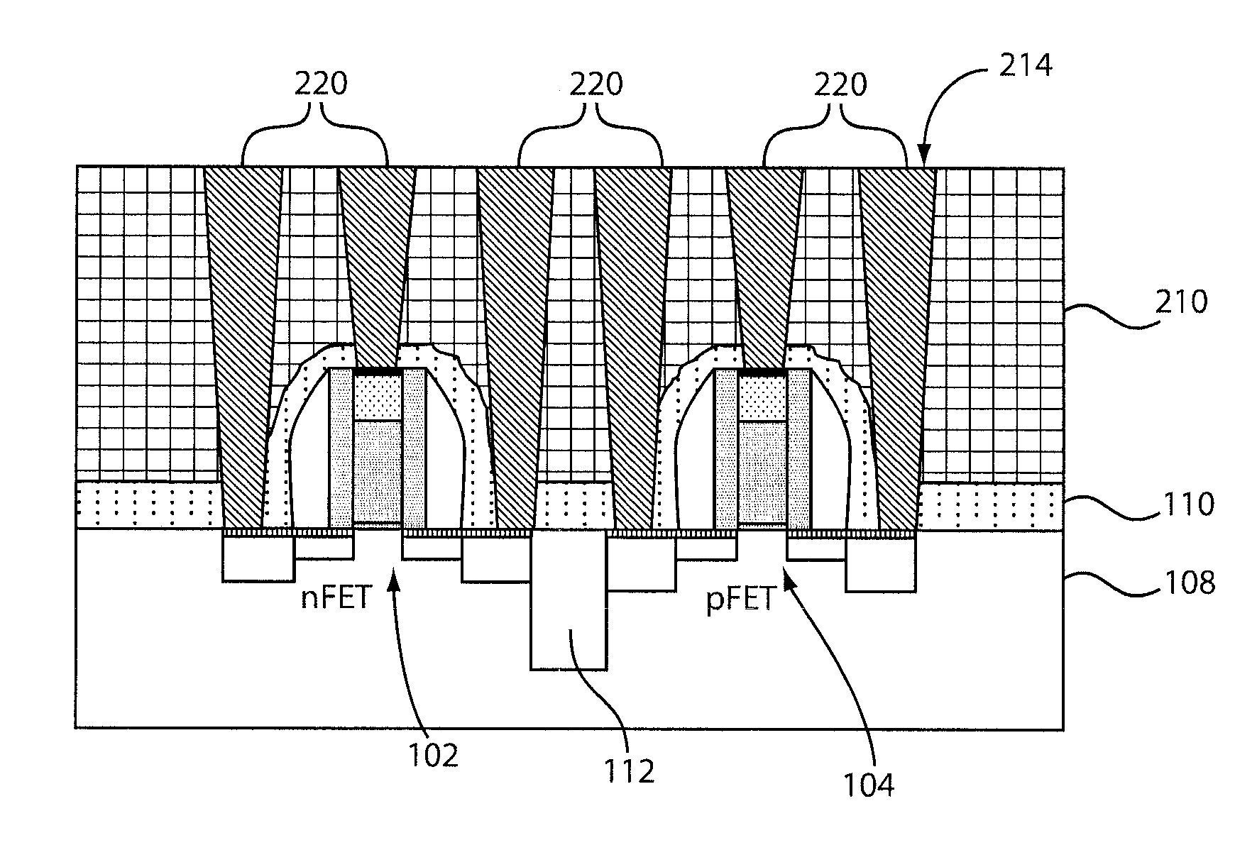
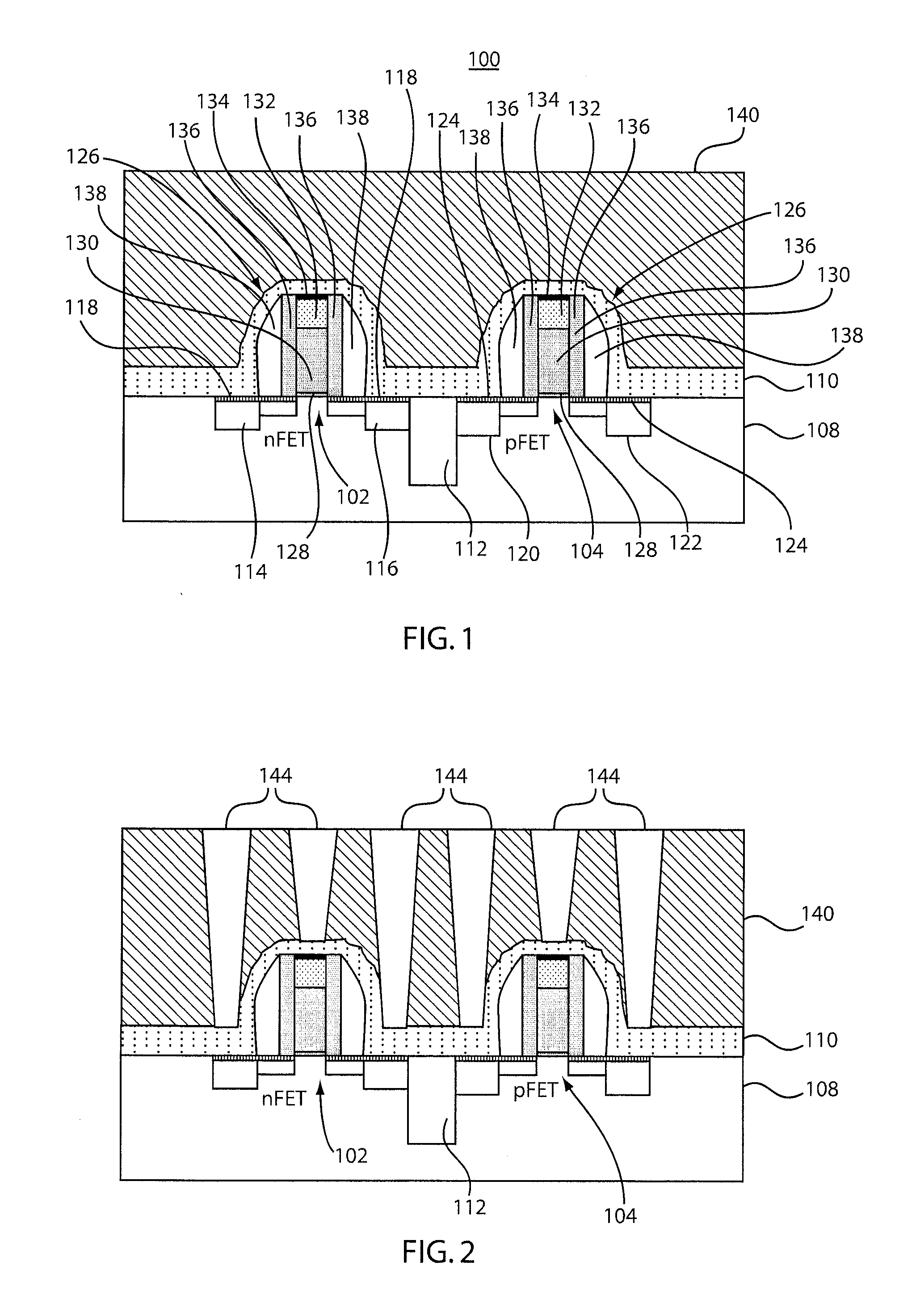
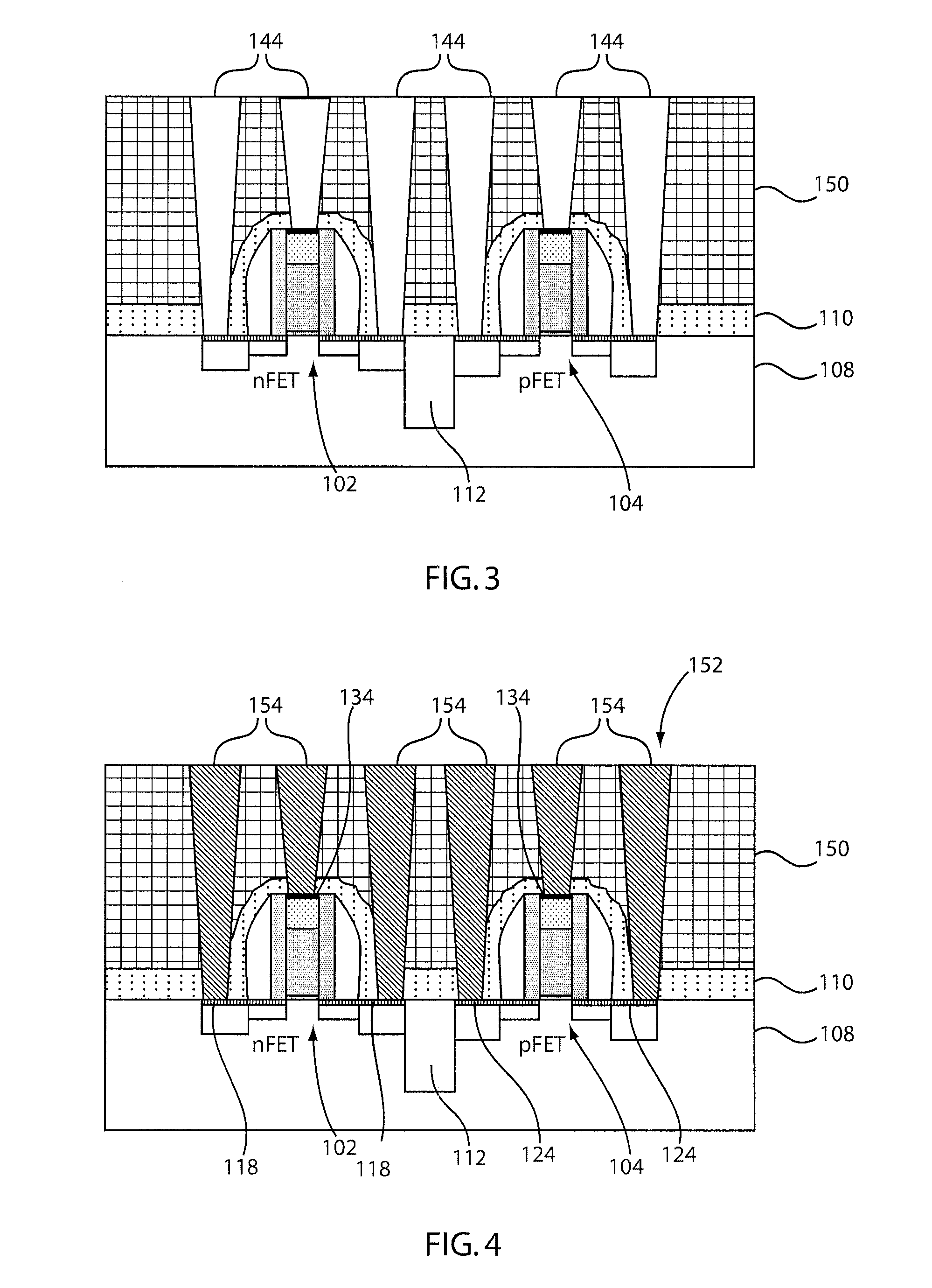
[0025]The present principles provide electrically conductive contact structures and methods for fabrication by direct patterning of the dielectric material or by an image reversal patterning technique. In particularly useful embodiments, new integration schemes are provided to form contacts. Nitride, oxide and resist mask stacks are replaced with a permanent antireflection coating and a patternable dielectric composition, which can be converted to a patterned and cured permanent dielectric layer. The patternable dielectric composition layer is developed to transfer a pattern, i.e., via and / or bars. The dielectric composition layer is cured into a permanent dielectric structural layer to replace the oxide / nitride dielectric stack. It should be understood that the patternable dielectric composition may be formed as the permanent dielectric layer upon deposition.

[0026]In some embodiments, drawbacks of conventional integration processes are avoided by, e.g., combining the functions of a...


PUM


Abstract

A contact structure includes a permanent antireflection coating formed on a substrate having contact pads. A patterned dielectric layer is formed on the antireflective coating. The patterned dielectric layer and the permanent antireflective coating form openings. The openings correspond with locations of the contact pads. Contact structures are formed in the openings to make electrical contact with the contacts pads such that the patterned dielectric layer and the permanent antireflective coating each have a conductively filled region forming the contact structures.

Description

RELATED APPLICATION INFORMATION[0001]This application is related to commonly assigned application Ser. No. ______ entitled: INTERCONNECT STRUCTURE AND METHOD FOR FABRICATING ON-CHIP INTERCONNECT STRUCTURES BY IMAGE REVERSAL (Attorney Docket Number YOR92011023US1 (163-393)), and commonly assigned application Ser. No. ______, entitled: SELF-ALIGNED AIRGAP INTERCONNECT STRUCTURES AND METHODS OF FABRICATION (Attorney Docket Number YOR92011022US1 (163-394)), both filed concurrently herewith and incorporated herein by reference.BACKGROUND[0002]1. Technical Field[0003]The present invention relates to semiconductor contact structures and fabrication methods, and in particular to contact structures made by direct patterning of dielectric material or by image reversal patterning.[0004]2. Description of the Related Art[0005]Typical conventional integration schemes for forming electrical contacts for transistors in a semiconductor chip include depositing a nitride stop layer on top of finished ...

Claims


Application Information

Patent Timeline
IPC IPC(8): H01L21/283H01L23/48
CPCH01L21/76814H01L21/76816H01L21/76825H01L21/76826H01L21/76828H01L21/76829H01L21/76832H01L2924/0002H01L21/0272H01L21/31058H01L21/311H01L21/283H01L2924/00H01L21/76897H01L21/76895H01L21/76805H01L21/76879H01L21/76808H01L21/76802H01L21/76877H01L21/0276
Inventor LIN, QINGHUANGZHANG, YING
Owner ALSEPHINA INNOVATIONS INC
Learn More