Lens array and optical module provided therewith
a technology of optical modules and arrays, applied in the field of lenses arrays and optical modules, can solve problems such as preventing the transmission of communication information, and achieve the effect of facilitating manufacturing
- Summary
- Abstract
- Description
- Claims
- Application Information
AI Technical Summary
Benefits of technology
Problems solved by technology
Method used
Image

Examples
embodiment 1
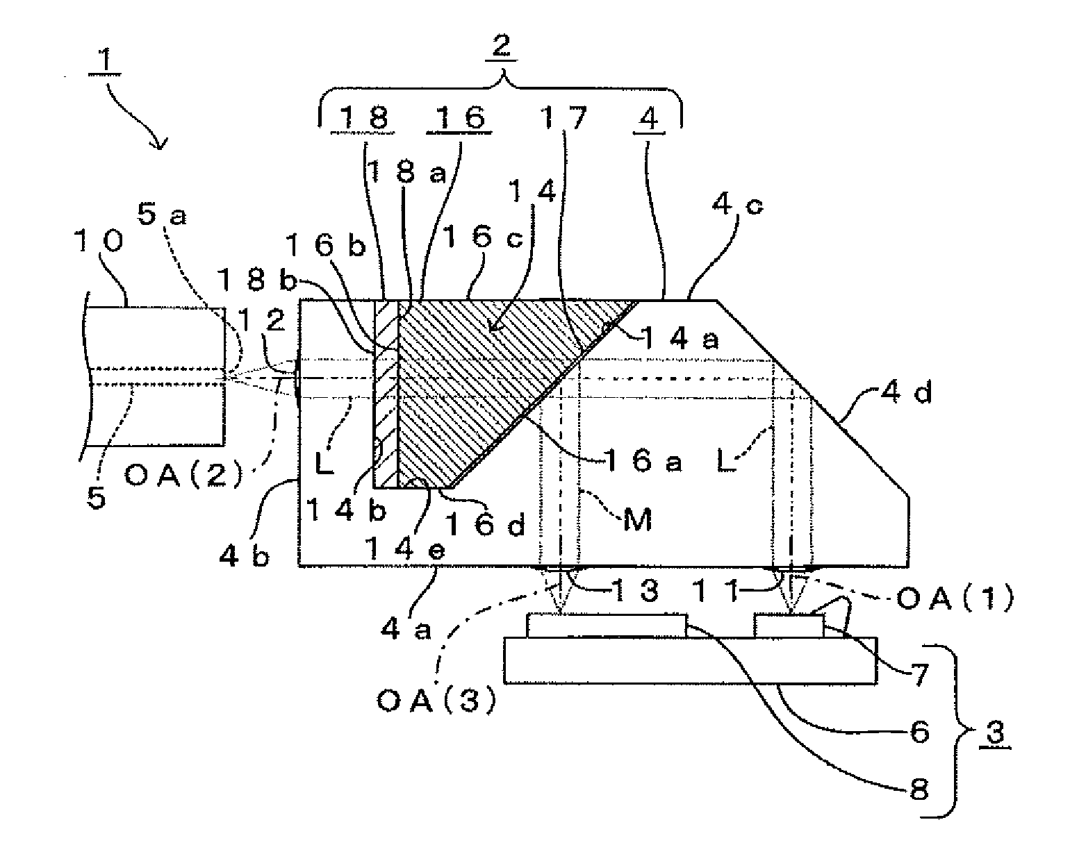
[0088]Embodiment 1 of a lens array and an optical module provided therewith according to the present invention will now be described with reference to FIGS. 1 to 6.
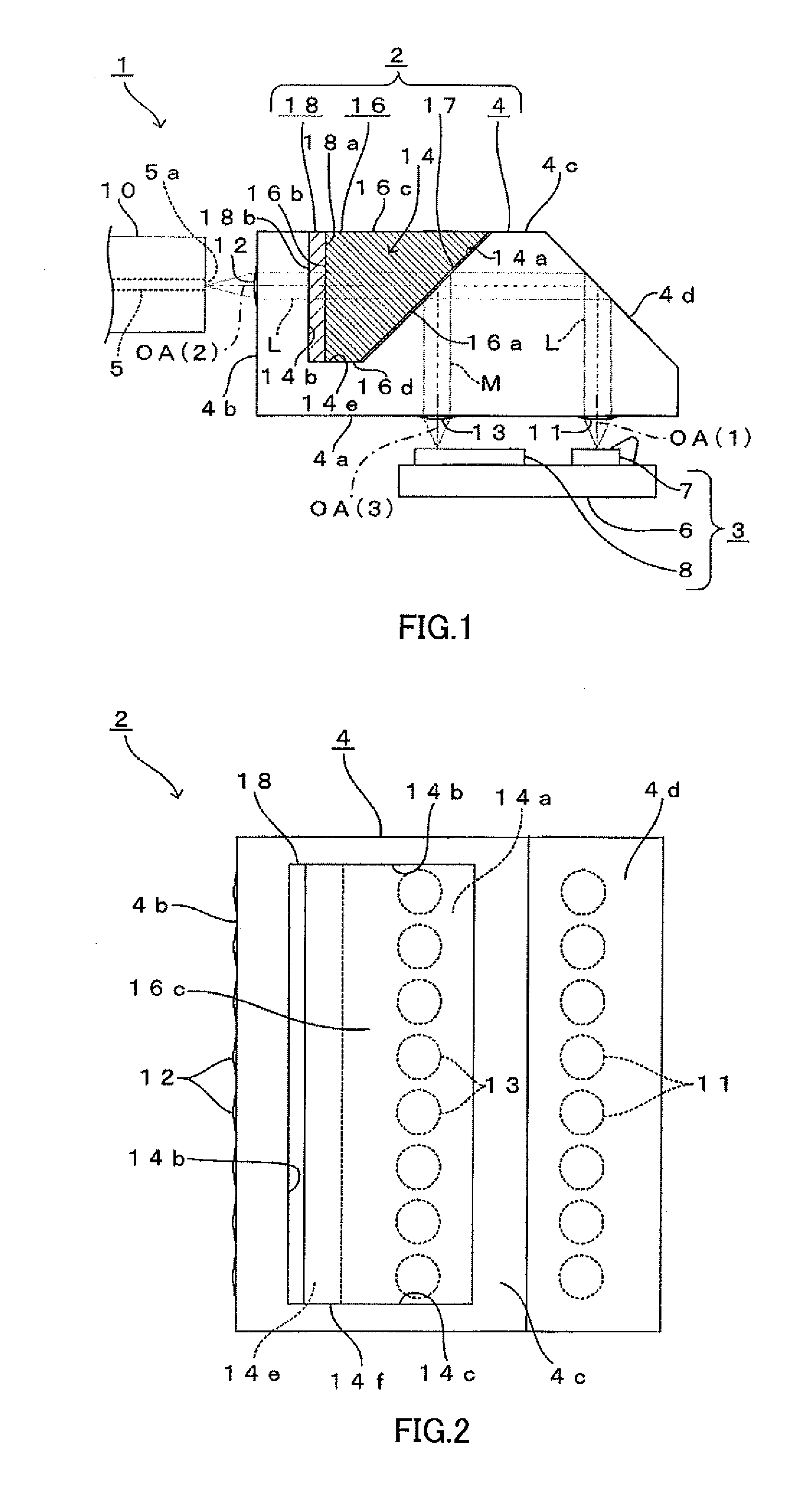
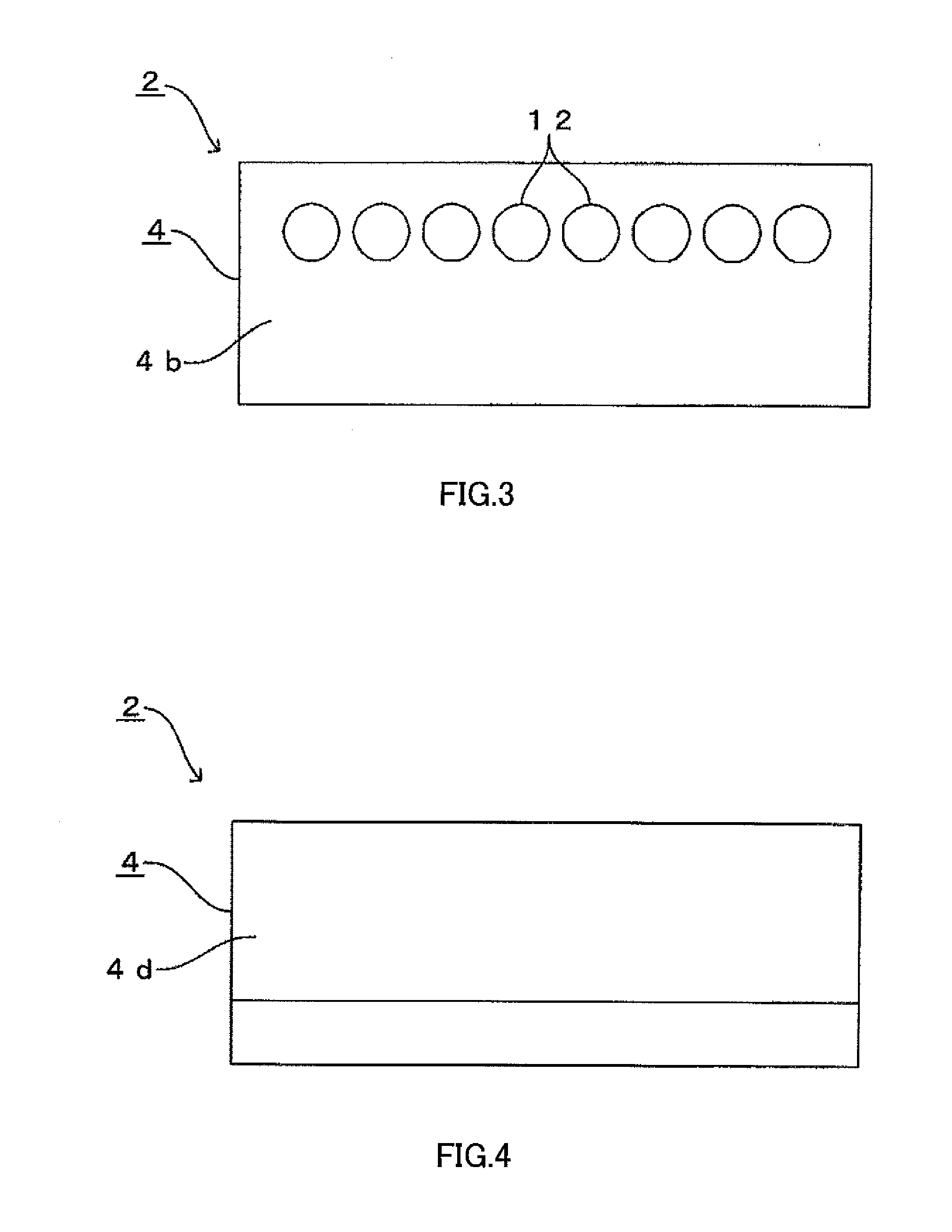
[0089]FIG. 1 is a configurational diagram schematically showing an overview of optical module 1 in this embodiment together with a longitudinal sectional view of lens array 2 in this embodiment. FIG. 2 is a plan view of lens array 2 shown in FIG. 1. FIG. 3 is a left side view of lens array 2 shown in FIG. 1. FIG. 4 is a right side view of lens array 2 shown in FIG. 1. FIG. 5 is a bottom view of lens array 2 shown in FIG. 1.
[0090]As shown in FIG. 1, lens array 2 in this embodiment is disposed between optoelectric converting device 3 and optical fiber 5.
[0091]Here, optoelectric converting device 3 includes a plurality of light emitting elements 7 that emit laser light L toward a surface of semiconductor substrate 6 facing lens array 2 in the direction perpendicular to this surface (upper direction in FIG. 1). Light emitting...
embodiment 2
[0136]Embodiment 2 of a lens array and an optical module provided therewith according to the present invention will now be described mainly on difference from Embodiment 1 with reference to FIGS. 7 to 12.
[0137]In this embodiment, elements having configurations identical or similar to those in FIGS. 1 to 6 will be described using the same reference signs as those of FIGS. 1 to 6.
[0138]FIG. 7 is a configurational diagram schematically showing an overview of optical module 21 in this embodiment together with a longitudinal sectional view of lens array 22 in this embodiment. FIG. 8 is a plan view of lens array 22 shown in FIG. 7. FIG. 9 is a left side view of FIG. 8. FIG. 10 is a right side view of FIG. 8. FIG. 11 is a bottom view of FIG. 8.
[0139]In this embodiment, as a difference from Embodiment 1, means is provided for mechanically positioning optoelectric converting device 3 and optical fiber 5 when optoelectric converting device 3 and optical fiber 5 are fixed to lens array 22.
[014...
embodiment 3
[0149]Embodiment 3 of a lens array and an optical module provided therewith according to the present invention will now be described mainly on difference from Embodiments 1 and 2 with reference to FIGS. 13 to 16.
[0150]In this embodiment, elements having configurations identical or similar to those in FIGS. 1 to 12 will be described using the same reference signs as those of FIGS. 1 to 12.
[0151]FIG. 13 is a configurational diagram schematically showing an overview of optical module 30 in this embodiment together with a longitudinal sectional view of lens array 31 in this embodiment. FIG. 14 is a plan view of lens array 31 shown in FIG. 13.
[0152]FIG. 15 is a right side view in FIG. 14.
[0153]As shown in FIG. 13, the configuration in this embodiment is similar to those in Embodiment 2 in that the side surfaces of concave part 14 extend upwardly from first optical surface 14a and second optical surface 14b, and filler 18 fills a space over top face 16c of prism 16.
[0154]However, this emb...
PUM
 Abstract
Description
Claims
Application Information
 - Generate Ideas
- Intellectual Property
- Life Sciences
- Materials
- Tech Scout
- Unparalleled Data Quality
- Higher Quality Content
- 60% Fewer Hallucinations
Browse by: Latest US Patents, China's latest patents, Technical Efficacy Thesaurus, Application Domain, Technology Topic, Popular Technical Reports.
© 2025 PatSnap. All rights reserved.Legal|Privacy policy|Modern Slavery Act Transparency Statement|Sitemap|About US| Contact US: help@patsnap.com