Microchip and Method of Manufacturing the Same

Active Publication Date: 2012-10-25
HORIBA LTD
View PDF0 Cites 9 Cited by
  • Summary
  • Abstract
  • Description
  • Claims
  • Application Information

AI Technical Summary

Benefits of technology

[0010]However, the welding through photoirradiation described in Japanese Patent Laying-Open No. 2006-310828 or the like has the following problems: In the case of bonding the light-transmitting substrate and the light-absorbing substrate to each other, the light is generally applied to the whole surface of the light-transmitting substrate. If the quantity of the light applied to bonded portions (contact portions) of the light-transmitting substrate and the light-absorbing substrate, however, the substrates are defectively bonded to each other. If the quantity of the applied

Problems solved by technology

However, the welding through photoirradiation described in Japanese Patent Laying-Open No. 2006-310828 or the like has the following problems: In the case of bonding the light-transmitting substrate and the light-absorbing substrate to each other, the light is generally applied to the whole surface of the light-transmitting substrate.
If the quantity of the light applied to bonded portions (contact portions) of the light-transmitting substrate and the light-absorbing substrate, however, the substrates are defectively bonded to each other.
If the quantity of the applied light is increased to an extent causing no defect on all bonded

Method used


Image

  • Microchip and Method of Manufacturing the Same
  • Microchip and Method of Manufacturing the Same
  • Microchip and Method of Manufacturing the Same

Examples


first embodiment

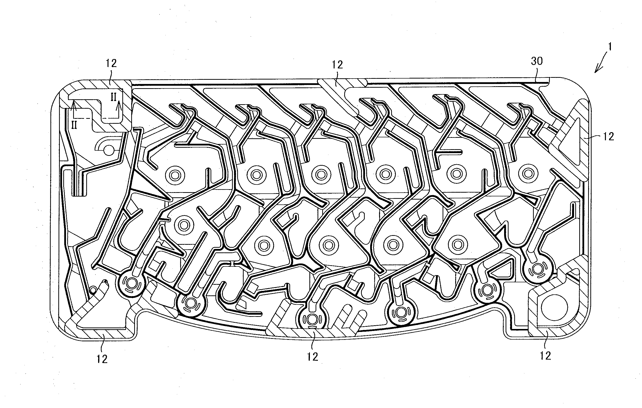
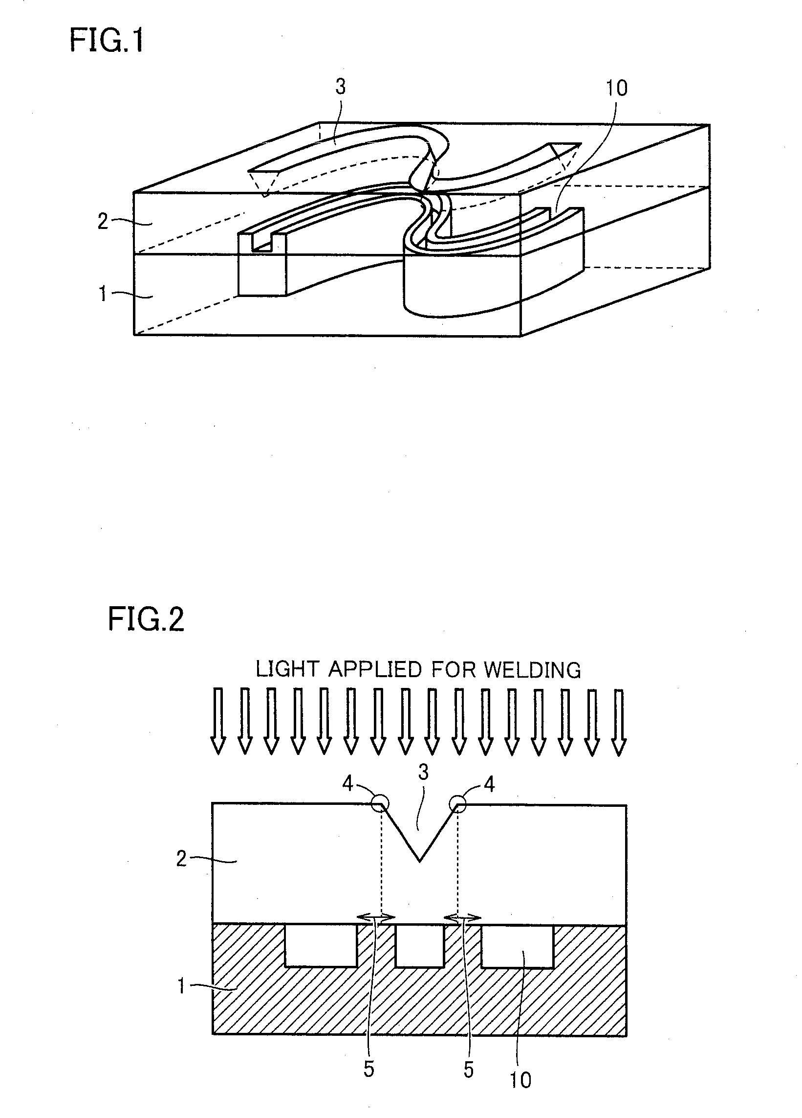
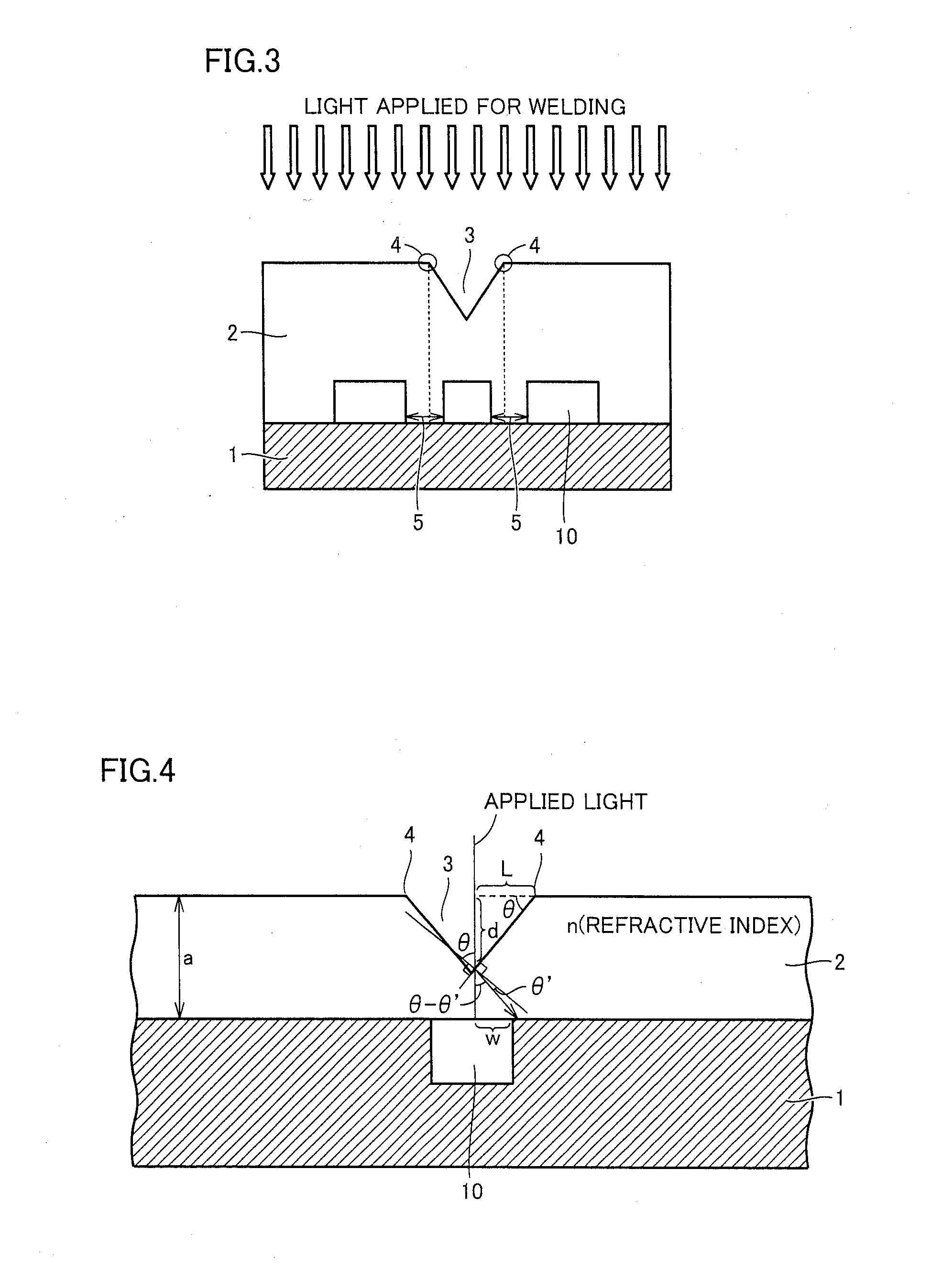
[0072]FIG. 1 is a perspective view conceptually showing a microchip according to a first embodiment of the present invention. As shown in FIG. 1, the microchip according to the first embodiment includes a light-absorbing first substrate 1 and a light-transmitting second substrate 2 bonded onto first substrate 1. First and second substrates 1 and 2 are bonded to each other by welding with light (a laser beam, lamplight or the like) applied to the side of second substrate 2. In other words, first and second substrates 1 and 2 are bonded to each other by melting a bonded surface of light-absorbing first substrate 1 with light transmitted through second substrate 2 to reach the interface between first and second substrates 1 and 2.

[0073]Referring to FIG. 1, a groove (recess portion) 10 constituting a fluid circuit is provided on a surface of first substrate 1 closer to second substrate 2, so that groove 10 and second substrate 2 form the fluid circuit (internal space). A groove 3, havin...

second embodiment

[0109]FIG. 11 is a schematic sectional view showing an exemplary microchip according to a second embodiment of the present invention. As shown in FIG. 11, the microchip according to the second embodiment includes a light-absorbing first substrate 1 and a light-transmitting second substrate 2 bonded onto first substrate 1. First and second substrates 1 and 2 are bonded to each other by welding with light (a laser beam, lamplight or the like) applied to the side of second substrate 2, similarly to the aforementioned first embodiment.

[0110]According to the second embodiment, a groove (recess portion) 10 constituting a fluid circuit is provided on a surface of light-transmitting second substrate 2 closer to first substrate 1, to form the fluid circuit (internal space) along with first substrate 1. A tapered structure portion 6 including protrusions having sections in the form of isosceles triangles and apical angles of 90° (tapered protrusions having sectional shapes tapered by 45° with...

third embodiment

[0121]A microchip according to a third embodiment of the present invention is constituted of a first substrate having a recess portion (groove) divided by partitions on at least a first surface and a second substrate bonded onto at least the first surface of the first substrate. A fluid circuit of the microchip includes a space constituted of the aforementioned recess portion (groove) and a surface of the second substrate. The surface (bonded to the first substrate) of the second substrate may be planar, or may be provided with a recess portion corresponding to that of the first substrate.

[0122]The microchip according to the third embodiment (and microchips according to fourth and fifth embodiments described later) may alternatively be constituted of at least three substrates. For example, the first substrate may have another recess portion also on a surface opposite to the second substrate, and a third substrate similar to the second substrate may be bonded to the side of this rece...


PUM

PropertyMeasurementUnit
Angleaaaaaaaaaa
Thicknessaaaaaaaaaa
Angleaaaaaaaaaa

Abstract

Provided are a microchip including a fluid circuit consisting of a space formed therein, a light-absorbing first substrate and a light-transmitting second substrate bonded onto the first substrate, and a groove, having a V-shaped section, extending parallelly to the fluid circuit on a surface of the second substrate opposite to the first substrate on a position immediately above at least part of the fluid circuit and a method of manufacturing the same.

Description

BACKGROUND OF THE INVENTION [0001]1. Field of the Invention[0002]The present invention relates to a microchip and a method of manufacturing the same. More specifically, it relates to a microchip useful for a μ-TAS (Micro Total Analysis System) or the like suitably used for biochemical testing of DNA, protein, a cell, immunity, blood etc., chemical synthesis and environmental analysis and a method of manufacturing the same.[0003]2. Description of the Background Art[0004]In recent years, importance of sensing, detecting or determining a biosubstance such as DNA (DeoxyriboNucleic Acid), an enzyme, an antibody, protein, a virus or a cell or a chemical substance has been increased in the fields of medical treatment, health, food and drug discovery, and there have been proposed various types of biochips and microchemical chips (the biochips and the microchemical chips are hereinafter generically referred to as microchips) allowing simple measurement thereof.[0005]A microchip of several cm...

Claims


Application Information

Patent Timeline
IPC IPC(8): F16L3/01B29C65/00B32B37/16
CPCB29C65/1435B29C66/30221B29C65/1635B29C65/1677B29C65/1693B29C65/8253B29C66/112B29C66/1122B29C66/114B29C66/30223B29C66/348B29C66/53461B29C66/73921B29C66/81267B29L2031/756B81C3/001B29C65/1493B81C2203/038B81B2201/0214B81C2201/019B01L3/502707B01L2200/0689B01L2300/0816B01L2300/0887B29C65/1477B29C66/8322B29C66/244B29C66/71B29C66/73365B29C66/73343B29C66/242Y10T137/8593B29C66/73161B29K2025/06B29K2009/06B29K2023/06B29K2023/12B29K2023/38B29K2033/12B29K2055/02B29K2059/00B29K2067/00B29K2067/003B29K2067/006B29K2069/00B29K2077/00B29K2083/00
Inventor MOMOSE, SHUNTAKEUCHI, HIROKI
Owner HORIBA LTD
Why Eureka
Try Eureka