Methods for etching through-silicon vias with tunable profile angles

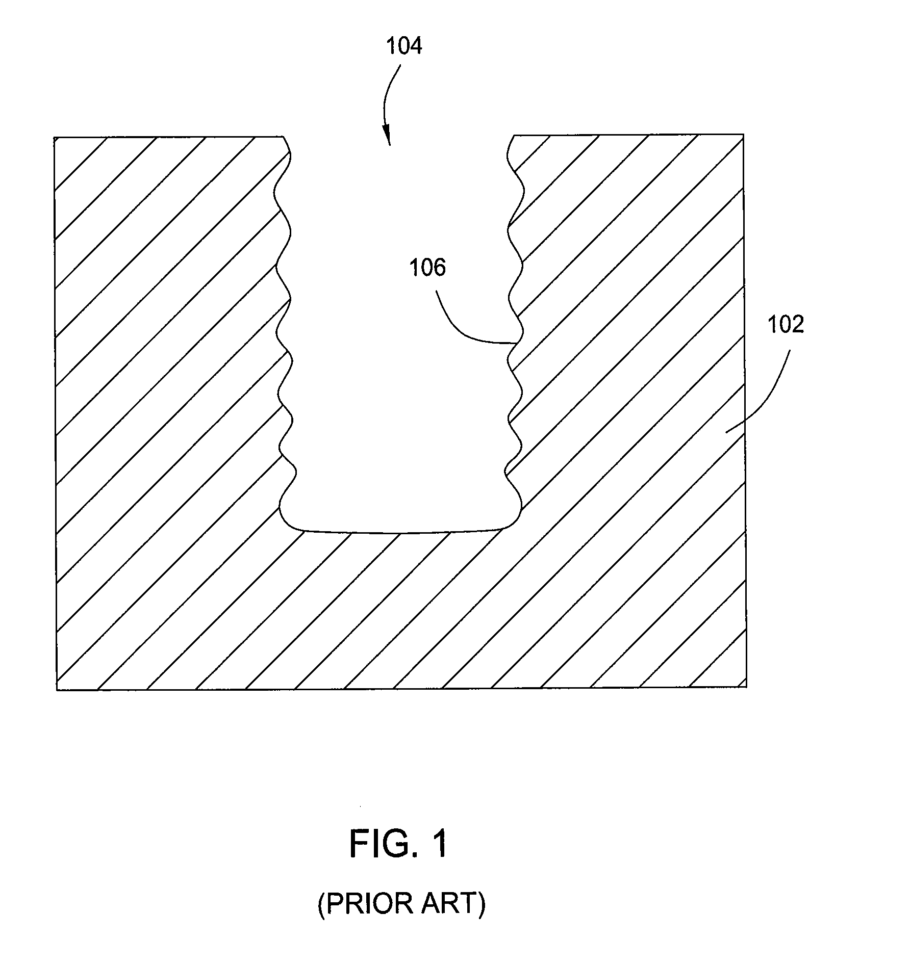
a technology of throughsilicon vias and profile angles, which is applied in the direction of semiconductor/solid-state device manufacturing, basic electric elements, electric devices, etc., can solve the problems of device failure, difficult sidewall surface, and strict control of etch profile, and achieve low process pressure, good sidewall profile, and high rf bias power

Active Publication Date: 2012-10-25
APPLIED MATERIALS INC
View PDF1 Cites 22 Cited by
  • Summary
  • Abstract
  • Description
  • Claims
  • Application Information

AI Technical Summary

Benefits of technology

[0009]The present disclosure provides methods for etching through-silicon vias (TSVs) in a substrate. The method employs a cyclic polymer passivation layer deposition, depassivation process and plasma etching process. By alternating the duration performed in the plasma etching process and the polymer passivation deposition process during the TSVs formation process, a good sidewall profile, via taper angle and via depth control may be obtained. In one embodiment, the good sidewall profile and via depth may be controlled by managing a relatively low process pressure and relatively high RF bias power during the polymer passivation deposition process and the depassivation process so as to maintain a desired anisotropic etching process until a desired sidewall profile and via depth is reached.
[0010]In one embodiment, a method for forming TSVs in a substrate includes performing a first etching process on a substrate in a processing chamber to form vias in the substrate, forming a polymer passivation layer on sidewall and a bottom of the vias formed in the substrate by supplying a polymer passivation gas mixture into the processing chamber while maintaining a process pressure at less than 200 mTorr for a first predetermined time period, removing a portion of the polymer passivation layer formed on the bottom of the vias by a depassivation gas mixture supplied into the processing chamber, and performing a second etching process to continue etching the vias with the polymer passivation layer remaining on the sidewalls of the vias for a second predetermined time period.
[0011]In another embodiment, a method for forming TSVs in a substrate includes performing a first etching process on a substrate in a processing chamber to form vias in the substrate, performing a polymer passivation deposition process on sidewalls and a bottom of the vias formed in the substrate while maintaining a process pressure at less than 200 mTorr for a first predetermined time period, performing a depassivation process to remove the polymer passivation layer from the bottom of the vias while maintaining a bias power to the substrate greater than about 150 watts during the depassivation process, and performing a second etching process to continue etching the vias with the polymer passivation layer remaining on the sidewalls of the vias for a second predetermined time period until a desired depth of the vias is reached
[0012]In one embodiment, a method for forming TSVs in a substrate includes supplying a first etching gas mixture into a processing chamber to partially form vias in a substrate disposed therein, wherein the process pressure within the processing chamber is maintained above 50 mTorr while partially forming the vias, supplying a polymer passivation gas mixture into the processing chamber to maintain the process pressure at less than about 200 mTorr until a polymer passivation layer with a desired thickness has formed in the vias, supplying a depassivation gas mixture into the processing chamber while maintaining a substrate bias power greater than about 150 watts until the polymer passivation layer formed on the bottom of the vias is removed, wherein the process pressure within the processing chamber is maintained between about 50 mTorr and about 150 mTorr while continuing to etch the vias, and supplying a second etching gas mixture into the processing chamber to continue etching the vias through the bottom exposed by the polymer passivation layer until the polymer passivation layer formed on the sidewalls of the vias are removed.

Problems solved by technology

Strict control of the etch profile is required for complex devices to perform satisfactorily.
Obtaining a controlled sidewall profile, where the taper angle range is from about 85 degrees to about 90 degrees in combination with a smooth sidewall surface has proved a difficult task in many instances.
Inaccurate control of the sidewall taper angles may cause difficulty for the following wiring and / or packaging process, thereby resulting in device failure or poor electrical performance.
Furthermore, etching process control for forming deep trenches or deep vias in a substrate is often challenging.
Improper etching process parameter control may result in defects formed in the resultant vias.
For example, improper control of RF power generated during the etching process may result in insufficient depth down to the bottom of the vias or render grass type defects on the bottom of the vias.

Method used


Image

  • Methods for etching through-silicon vias with tunable profile angles
  • Methods for etching through-silicon vias with tunable profile angles
  • Methods for etching through-silicon vias with tunable profile angles

Examples


Embodiment Construction

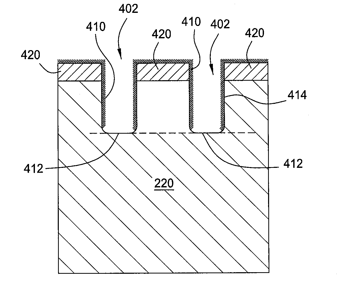
[0019]The present disclosure provides methods for etching through-silicon vias (TSVs) in a substrate. The method employs a protective cyclic polymer passivation deposition, depassivation process and plasma etching process. By alternating the duration of the plasma etching process and polymer passivation deposition process during the TSVs formation process, a good sidewall profile and via depth control may be obtained. In one embodiment, the good sidewall profile and via depth may be controlled by maintaining a relatively low process pressure and relatively high RF bias power during the polymer passivation deposition process so as to maintain a desired anisotropic etching process until a desired sidewall profile and via depth is reached.

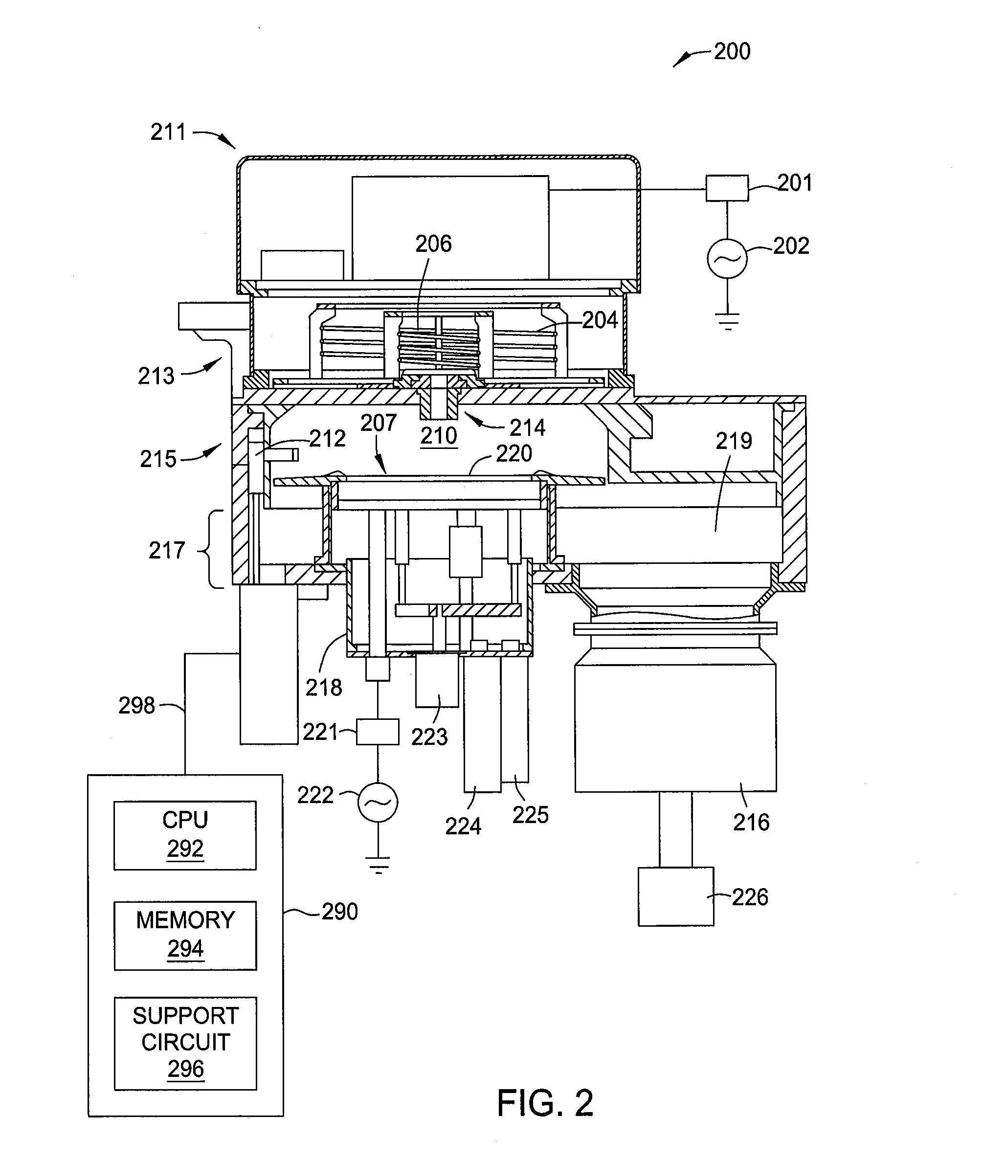
[0020]FIG. 2 depicts a schematic isometric view of a processing chamber 200 that may be used in conjunction with embodiments of the present invention to perform a TSV etching process. The TSV etching process may be practiced in a DPS II TSV processing...


PUM


Abstract

The present disclosure provides methods for etching through-silicon vias (TSVs) in a substrate. The method employs a cyclic polymer passivation layer deposition, depassivation process and plasma etching process. By alternating the duration performed in the plasma etching process and the polymer passivation deposition process during the TSVs formation process, a good sidewall profile and via depth control may be obtained.

Description

CROSS REFERENCE TO RELATED APPLICATION[0001]This application claims benefit of U.S. Provisional Patent Application No. 61 / 478,733, filed Apr. 25, 2011, which is incorporated by reference in its entirety.BACKGROUND[0002]1. Field[0003]Embodiments of the invention generally relate to a method for etching through-silicon vias (TSVs) with tunable profile angles while maintaining desired etching rates.[0004]2. Description of the Related Art[0005]Deep recessed structure etching is one of the principal technologies currently being used to fabricate semiconductor and microstructure devices. Strict control of the etch profile is required for complex devices to perform satisfactorily. Obtaining a controlled sidewall profile, where the taper angle range is from about 85 degrees to about 90 degrees in combination with a smooth sidewall surface has proved a difficult task in many instances.[0006]Through-silicon vias (TSVs) with a sidewall taper angle ranging from about 85 degrees to about 90 degr...

Claims


Application Information

Patent Timeline
Patent Type & Authority Applications(United States)
IPC IPC(8): H01L21/302
CPCH01L21/76898H01L21/30655
Inventor BAJAJ, PUNEETLIU, TONGSIRAJUDDIN, KHALID MOHIUDDIN
Owner APPLIED MATERIALS INC
Why Eureka
Try Eureka