Semiconductor device

a technology of semiconductors and devices, applied in the direction of semiconductor devices, basic electric elements, electrical appliances, etc., can solve problems such as resistance and voltage rise, and achieve the effects of reducing resistance, improving current breaking capability, and lowering voltag

Active Publication Date: 2012-11-01
MITSUBISHI ELECTRIC CORP
View PDF1 Cites 13 Cited by
  • Summary
  • Abstract
  • Description
  • Claims
  • Application Information

AI Technical Summary

Benefits of technology

[0007]To solve the problem as described above, it is an object of the present invention to obtain a semiconductor device that can lower ON voltage while improving a current breaking capability during turn-off operations.
[0008]According to the present invention, a semiconductor device comprises: a transistor region including an IGBT having a gate electrode and an emitter electrode; a termination region placed around the transistor region; an extraction region placed between the transistor and the termination region and extracting redundant carriers, wherein a P-type layer is placed on an N-type drift layer in the extraction region, the P-type layer is connected to the emitter electrode, a dummy gate electrode is placed via an insulation film on the P-type layer, the dummy gate electrode is connected to the gate electrode, life time of carriers in the termination region is shorter than life time of carriers in the transistor region and the extraction region.
[0009]The present invention makes it possible to lower ON voltage while improving a current breaking capability during turn-off operations.

Problems solved by technology

Therefore, when lattice defect is introduced in the extraction region, there is a problem of the elevation of ON voltage (ON resistance).

Method used


Image

  • Semiconductor device
  • Semiconductor device
  • Semiconductor device

Examples


first embodiment

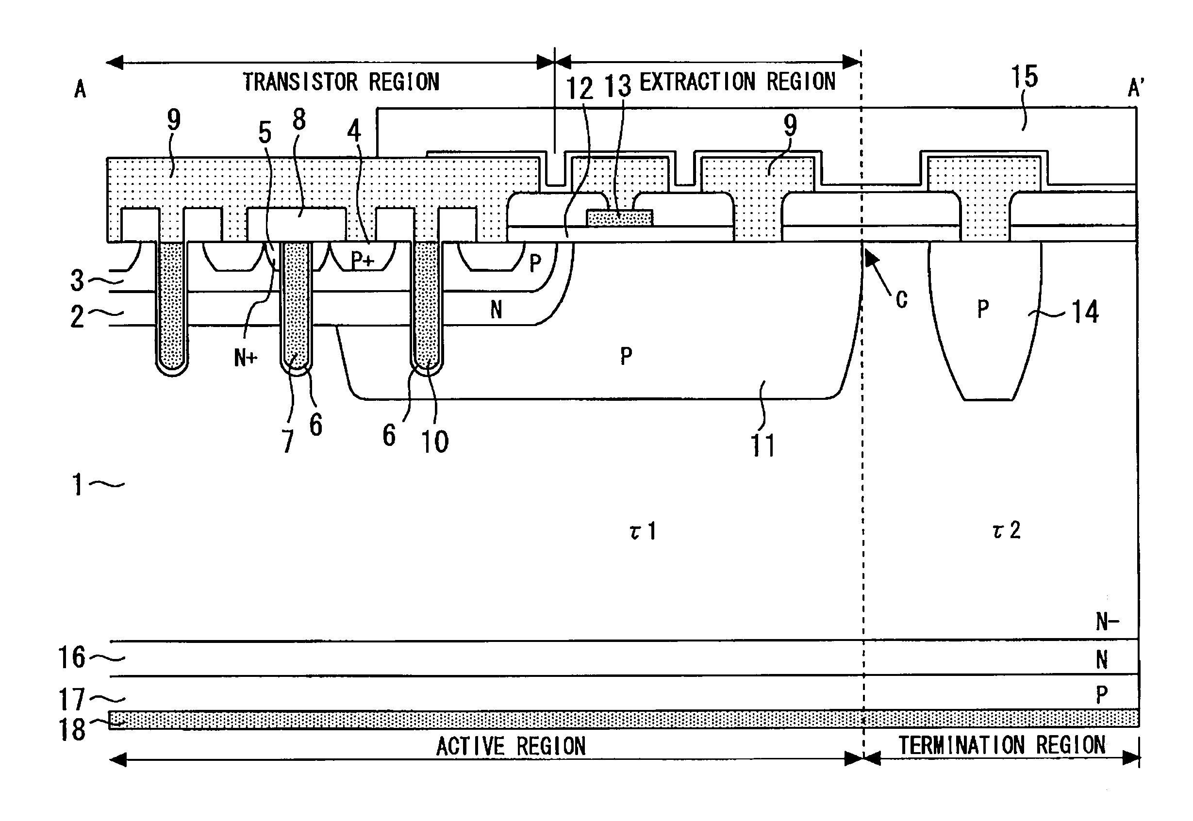
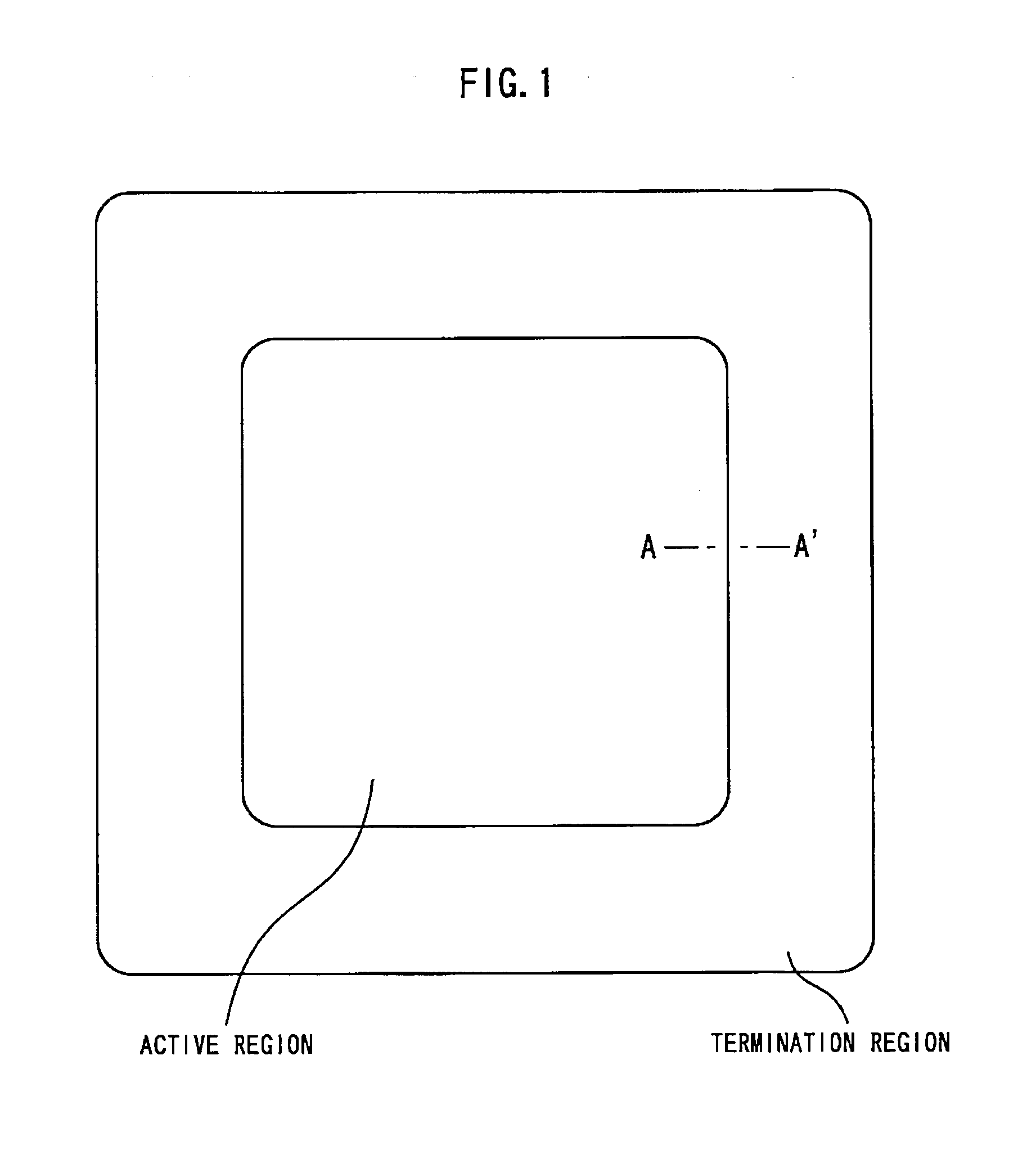
[0027]FIG. 1 is a top view showing a semiconductor device according to the first embodiment of the present invention. The semiconductor device is a power device of high withstand voltage (600 V or higher) having an IGBT. A termination region is placed around an active region. If a voltage is applied between a collector and an emitter when the IGBT is turned off, a depletion layer extends laterally in the termination region. Therefore, by forming the termination region, withstand voltage can be maintained. In addition, when the IGBT is ON, although a principal current flows in the active region, no principal current flows in the termination region.

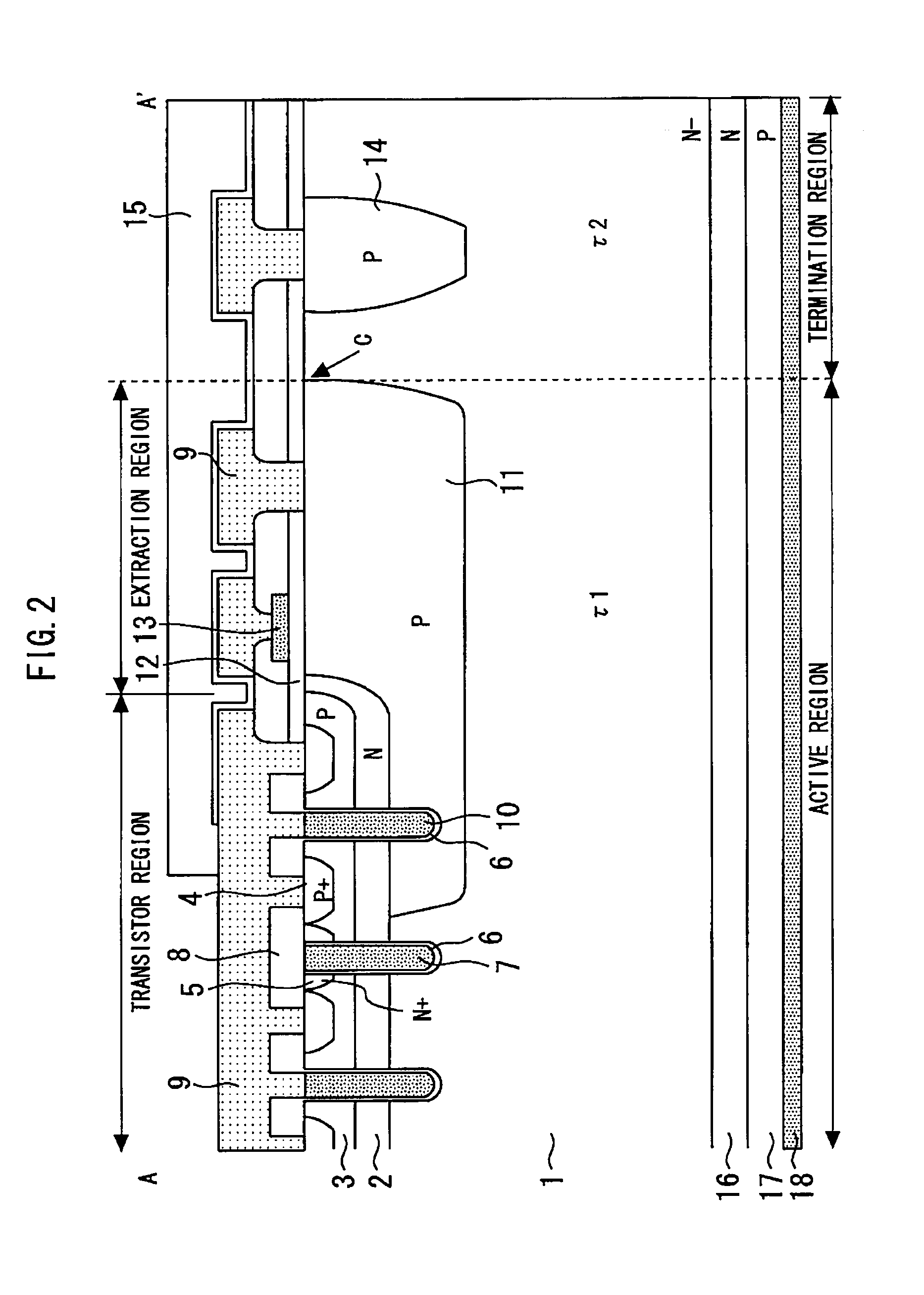
[0028]FIG. 2 is a sectional view taken along the line A-A′ in FIG. 1. The active region includes a transistor region having a plurality of trench-gate-type IGBT structure, and an extraction region placed between the transistor region and the termination region.

[0029]In the transistor region, an N-type charge accumulation layer 2 is formed o...

second embodiment

[0046]FIG. 12 is a sectional view showing a semiconductor device according to the second embodiment of the present invention. In the transistor region and the extraction region, an N-type buffer layer 16 is formed under an N−-type drift layer 1, and a P-type collector layer 17 is formed thereunder. In the termination region, an N-type buffer layer 19 is formed under the N−-type drift layer 1. A collector electrode 18 is directly connected to the P-type collector layer 17 and the N-type buffer layer 19. In other words, the N-type buffer layer 19 in the termination region is directly contacted (short-circuited) to the collector electrode 18.

[0047]Next, the effect of the second embodiment will be described comparing to a comparative example. In the comparative example, the P-type collector layer 17 is formed also in the termination region, and the N-type buffer layer 19 is not directly contacted to the collector electrode 18.

[0048]FIG. 13 is a diagram showing an evaluative circuit when...

third embodiment

[0052]FIG. 15 is a sectional view showing a semiconductor device according to the third embodiment of the present invention. In the transistor region and the extraction region, an N-type buffer layer 16 is formed under the N−-type drift layer 1. In the termination region, an N+-type buffer layer 20 is formed under the N−-type drift layer 1. A P-type collector layer 17 is formed under the N-type buffer layer 16 and the N+-type buffer layer 20. A collector electrode 18 is connected to the P-type collector layer 17. The impurity concentration of the N+-type buffer layer 20 is higher than the impurity concentration of the N-type buffer layer 16.

[0053]In the third embodiment, an N+-type buffer layer 20 having a high impurity concentration is formed in the termination region. Thereby, since hole implantation from the P-type collector layer 17 is suppressed in the termination region during the turn-off operation of the IGBT, depletion from the P-type layer 11 to the collector side is accel...


PUM


Abstract

A semiconductor device includes: a transistor region including an IGBT having a gate electrode and an emitter electrode; a termination region placed around the transistor region; and an extraction region placed between the transistor and the termination region and extracting redundant carriers. A P-type layer is placed on an N-type drift layer in the extraction region. The P-type layer is connected to the emitter electrode. A dummy gate electrode is placed via an insulation film on the P-type layer. The dummy gate electrode is connected to the gate electrode. Life time of carriers in the termination region is shorter than life time of carriers in the transistor region and the extraction region.

Description

BACKGROUND OF THE INVENTION[0001]1. Field of the Invention[0002]The present invention relates to a semiconductor device having an IGBT (Insulated Gate Bipolar Transistor).[0003]2. Background Art[0004]A semiconductor device having an IGBT is used as a power device of high withstand voltage (600 V or higher). As such a semiconductor device, there has been proposed a semiconductor device wherein an extraction region is placed between a transistor region having the IGBT and a termination region placed around the transistor region (for example, refer to the p-layer 4′ in FIG. 1 of Japanese Patent Application Laid-Open No. 6-21358). By the configuration of the extraction region, redundant carriers (holes) can be extracted during turn-off operation.[0005]In the semiconductor device according to Japanese Patent Application Laid-Open No. 6-21358, lattice defect is introduced into the termination region and the extraction region. Since the carrier concentration during turn-off operation can b...

Claims


Application Information

Patent Timeline
Patent Type & Authority Applications(United States)
IPC IPC(8): H01L29/739
CPCH01L29/7397H01L29/0619
Inventor SADAMATSU, KOJICHEN, ZENAKAMURA, KATSUMI
Owner MITSUBISHI ELECTRIC CORP
Why Eureka
Try Eureka