Resistance changing element, semiconductor device, and method for forming resistance change element
a technology of resistance change element and resistance change element, which is applied in the direction of resistive material coating, bulk negative resistance effect device, solid-state device, etc., can solve the problems of dielectric breakdown voltage adversely becoming low, and initial set voltage adversely becoming too high, so as to reduce the forming voltage and reduce the film thickness of the ion conducting layer , the effect of adversely affecting the operation voltag
- Summary
- Abstract
- Description
- Claims
- Application Information
AI Technical Summary
Benefits of technology
Problems solved by technology
Method used
Image

Examples
first embodiment
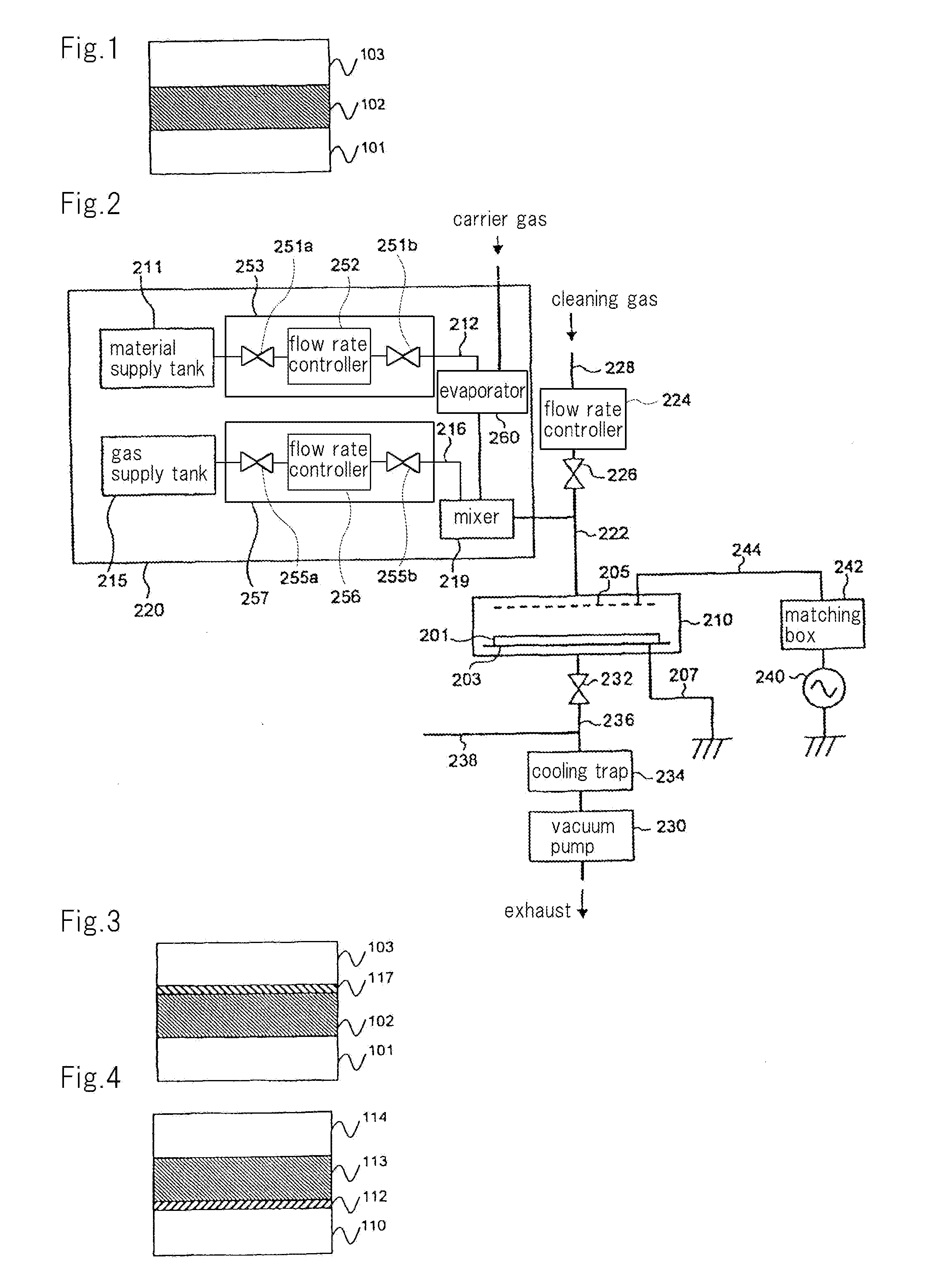
[0057]Here, with reference to the accompanying drawings, a semiconductor device according to a first embodiment of the present invention will be described. FIG. 1 is a sectional view schematically showing an example of a structure of the semiconductor device according to this embodiment.
[0058]As shown in FIG. 1, the semiconductor device according to this embodiment has first electrode 101, porous film 102, and second electrode 103. Formed successively on first electrode 101 are porous film 102 and second electrode 103. First electrode 101 is composed of metals whose main component is copper. Porous film 102 contains silicon (Si), oxygen (O), and carbon (C) as constituent elements.
[0059]Here, first electrode 101 and second electrode 103 of the semiconductor device according to this embodiment will be described. First electrode 101 is composed of metals containing copper. First electrode 101 serves to supply copper ions to the ion conducting layer. First electrode 101 may contain impu...
second embodiment
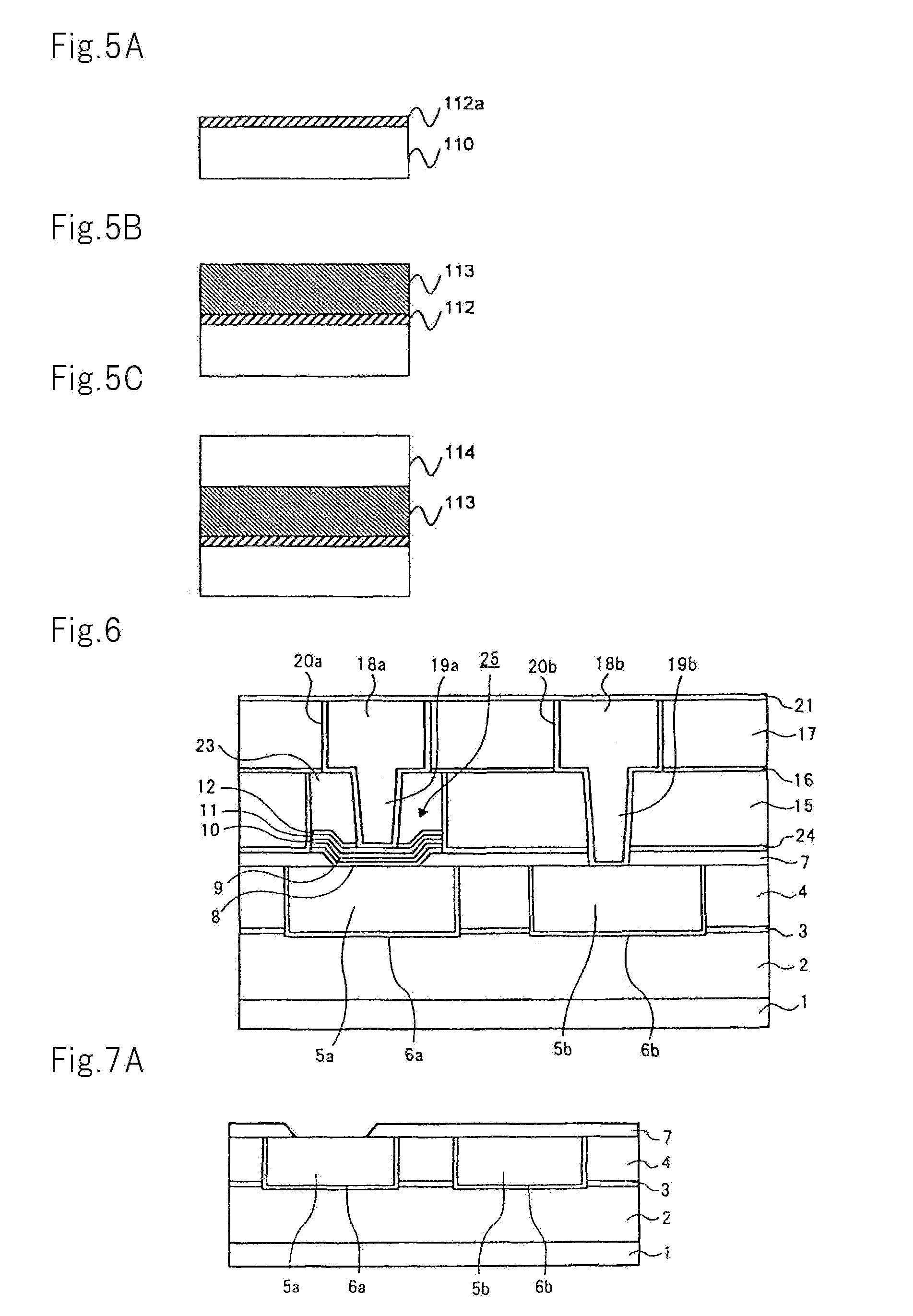
[0110]Next, the structure of a resistance changing element according to a second embodiment will be described. FIG. 4 is a sectional view showing an example of a structure of the resistance changing element according to this embodiment.
[0111]As shown in FIG. 4, the resistance changing element according to this embodiment has first electrode 110, titanium oxide film 112, ion conducting layer 113, and second electrode 114. Formed successively on first electrode 110 are titanium oxide film 112, ion conducting layer 113, and second electrode 114.
[0112]Next, with reference to FIG. 5A to FIG. 5C, a method that manufactures the resistance changing element according to this embodiment will be described in detail. It should be noted that the present invention is not limited to the following embodiment.
[0113]In the following, with reference to FIG. 5, an example of the method for manufacturing the resistance changing element according to the present invention will be described in brief. First...
third embodiment
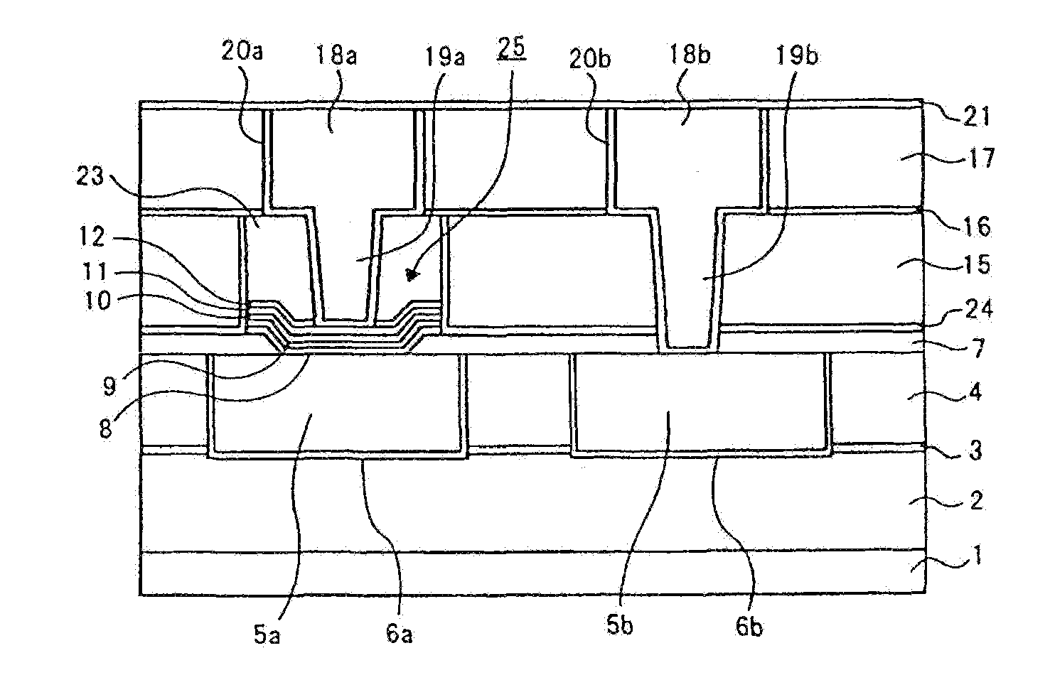
[0138]Next, with reference to the accompanying drawings, a semiconductor device according to a third embodiment of the present invention will be described. According to this embodiment, a resistance changing element is formed in a multi-layered wiring layer of the semiconductor device.
[0139]FIG. 6 is a partial sectional view schematically showing a structure of the semiconductor device according to this embodiment.
[0140]Resistance changing element 25 of the semiconductor device according to this embodiment has first wire 5a that serves as a lower electrode; titanium oxide film 8; ion conducting layer 9; first upper electrode 10; and second upper electrode 11.
[0141]In the semiconductor device according to this embodiment, hard mask film 23 that is a thick film is formed on a laminate of first upper electrode 10, second upper electrode 11, and hard mask film 12. The side surfaces of titanium oxide film 8, ion conducting layer 9, first upper electrode 10, second upper electrode 11, har...
PUM
 Abstract
Description
Claims
Application Information
 - R&D
- Intellectual Property
- Life Sciences
- Materials
- Tech Scout
- Unparalleled Data Quality
- Higher Quality Content
- 60% Fewer Hallucinations
Browse by: Latest US Patents, China's latest patents, Technical Efficacy Thesaurus, Application Domain, Technology Topic, Popular Technical Reports.
© 2025 PatSnap. All rights reserved.Legal|Privacy policy|Modern Slavery Act Transparency Statement|Sitemap|About US| Contact US: help@patsnap.com