Nonvolatile memory device using a tunnel oxide layer and oxygen blocking layer as a current limiter element

a technology of oxygen blocking layer and tunnel oxide layer, which is applied in static storage, electrical appliances, instruments, etc., can solve the problems of damage to the switching characteristics of the variable resistance layer, and achieve the effects of reducing the forming voltage of the device, reducing the switching current of the formed device, and reducing the performance variation

Active Publication Date: 2013-08-22
SANDISK TECH LLC +2
View PDF8 Cites 13 Cited by
  • Summary
  • Abstract
  • Description
  • Claims
  • Application Information

AI Technical Summary

Benefits of technology

[0012]Embodiments of the invention generally relate to a resistive switching nonvolatile memory device having a passive current limiter layer and a barrier layer structure disposed between at least one of the electrodes and a variable resistance layer formed in the nonvolatile memory device. The resistive switching memory elements may be formed as part of a high-capacity nonvolatile memory integrated circuit, which can be used in various electronic devices, such as digital cameras, mobile telephones, handheld computers, and music players. The resistive switching nonvolatile memory device comprises a variable resistance layer and current limiter layer that are configured to adjust the nonvolatile memory device's performance, such as lowering the formed device's switching currents and reducing the device's forming voltage, and reducing the performance variation from one formed device to another. A separation layer is provided between the variable resistance layer and the current limiting layer to prevent the diffusion of mobile ions between the two layers, and thus damaging the switching characteristics of the variable resistance layer. Mobile ions may include one or more elements found in the adjacent layers. In one example, the mobile ions found in the variable resistance layer may be oxygen ions (O2−).
[0013]The present invention may provide a nonvolatile memory element, comprising a first electrode layer, a second electrode layer, a variable resistance layer comprising a metal oxide disposed between the first electrode layer and the second electrode layer. A separation layer that inhibits the flow of oxygen ions is disposed between the variable resistance layer and a current limiter layer. The thickness of the separation layer is greater than the average diffusion length of the oxygen ions within the separation layer.
[0014]In one embodiment, the separation layer has an electrical resistance that is less than one fifth of the combined electrical resistance of the separation layer, the variable resistance layer, the current limiting layer and the two electrode layers.
[0015]Embodiments of the present invention may further provide a method of forming a nonvolatile memory element including depositing a first electrode layer, a second electrode layer, and a variable resistance layer. The method further includes depositing a current limiting layer and a separation layer. The separation layer is disposed between the variable resistance layer and the current limiting layer. The thickness of the separation layer is greater than the average diffusion length of the oxygen ions within the separation layer. The separation layer has an electrical resistance that is less than one fifth of the combined electrical resistance of the separation layer, the variable resistance layer, the current limiting layer and the two electrode layers.

Problems solved by technology

A separation layer is provided between the variable resistance layer and the current limiting layer to prevent the diffusion of mobile ions between the two layers, and thus damaging the switching characteristics of the variable resistance layer.

Method used


Image

  • Nonvolatile memory device using a tunnel oxide layer and oxygen blocking layer as a current limiter element
  • Nonvolatile memory device using a tunnel oxide layer and oxygen blocking layer as a current limiter element
  • Nonvolatile memory device using a tunnel oxide layer and oxygen blocking layer as a current limiter element

Examples


Embodiment Construction

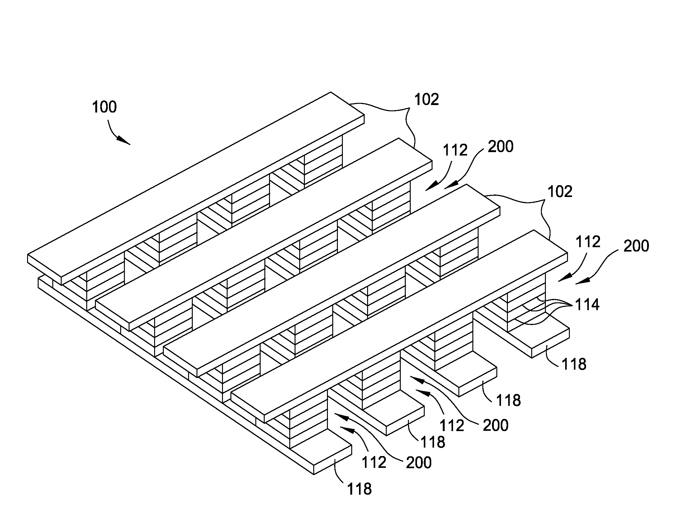
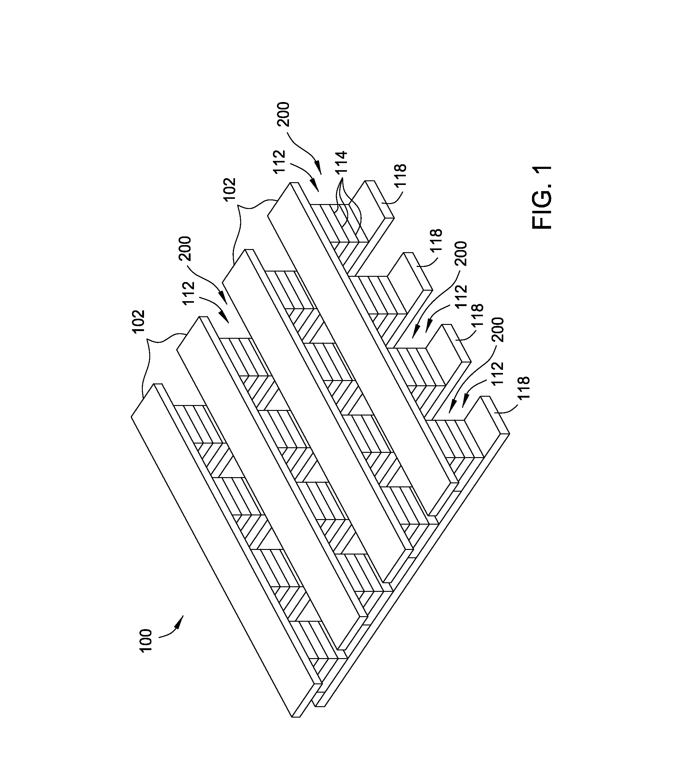
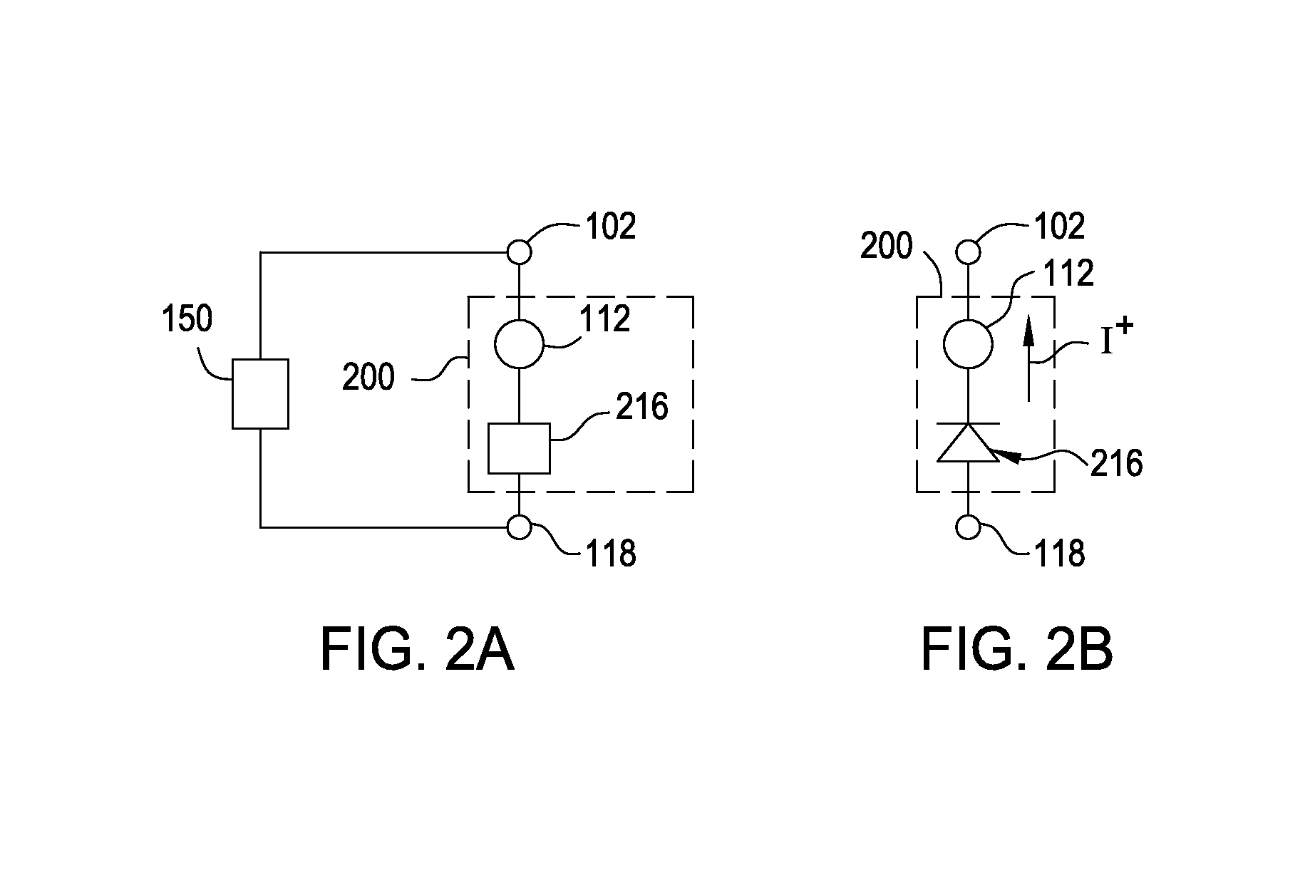
[0031]Embodiments of the invention generally include a method of forming a nonvolatile memory device that contains a resistive switching memory element that has an improved device switching performance and increased usable lifetime, due to the addition of a current limiting component disposed therein. In one embodiment, the current limiting component comprises a tunnel oxide current limiting layer together with a separation layer that acts as an oxygen barrier layer. The electrical properties of the formed current limiting layer are configured to lower the current flow through the variable resistance layer by adding a fixed series resistance in the formed nonvolatile resistive switching memory device. It is generally desirable to form the current limiting layer so that its material and electrical properties will not degrade or breakdown during the often high current “burn-in” type device preparation steps, such as the “electrical forming” process, and also during normal repetitive o...


PUM


Abstract

Embodiments of the invention include a method of forming a nonvolatile memory device that contains a resistive switching memory element with improved device switching performance and lifetime, due to the addition of a current limiting component. In one embodiment, the current limiting component comprises a resistive material configured to improve the switching performance and lifetime of the resistive switching memory element. The electrical properties of the current limiting layer are configured to lower the current flow through the variable resistance layer during the logic state programming steps by adding a fixed series resistance in the resistive switching memory element found in the nonvolatile memory device. In one embodiment, the current limiting component comprises a tunnel oxide layer that is a current limiting material and an oxygen barrier layer that is an oxygen deficient material disposed within a resistive switching memory element in a nonvolatile resistive switching memory device.

Description

BACKGROUND OF THE INVENTION[0001]1. Field of the Invention[0002]This invention relates to nonvolatile memory elements, and more particularly, to methods for forming resistive switching memory elements used in nonvolatile memory devices.[0003]2. Description of the Related Art[0004]Nonvolatile memory elements are used in systems in which persistent storage is required. For example, digital cameras use nonvolatile memory cards to store images and digital music players use nonvolatile memory to store audio data. Nonvolatile memory is also used to persistently store data in computer environments.[0005]Nonvolatile memory is often formed using electrically-erasable programmable read only memory (EEPROM) technology. This type of nonvolatile memory contains floating gate transistors that can be selectively programmed or erased by application of suitable voltages to their terminals.[0006]As fabrication techniques improve, it is becoming possible to fabricate nonvolatile memory elements with i...

Claims


Application Information

Patent Timeline
Patent Type & Authority Applications(United States)
IPC IPC(8): H01L47/00H01L21/02
CPCH01L45/08H01L45/1233G11C2213/51H01L45/146H01L45/16H01L45/1246H10N70/24H10N70/801H10N70/828H10N70/011H10N70/8833H10N70/826
Inventor TENDULKAR, MIHIRHASHIM, IMRANWANG, YUN
Owner SANDISK TECH LLC
Why Eureka
Try Eureka