Memory system and error correction method

a memory system and error correction technology, applied in the field of memory system and error correction method, can solve the problems of all types of eeprom and flash memory device, flash memory device may also become worn out,

Active Publication Date: 2012-11-08
SAMSUNG ELECTRONICS CO LTD
View PDF6 Cites 37 Cited by
  • Summary
  • Abstract
  • Description
  • Claims
  • Application Information

AI Technical Summary

Benefits of technology

[0022]Spatially relative terms, such as “beneath”, “below”, “lower”, “under”, “above”, “upper” and the like, may be used herein for ease of description to describe one element or feature's relationship to another element(s) or feature(s) as illustrated in the figures. It will be understood that the spatially relative terms are intended to encompass different orientations of the device in use or operation in addition to the orientation depicted in the figures. For example, if the device in the figures is turned over, elements described as “below” or “beneath” or “under” other elements or features would then be oriented “above” the other elements or features. Thus, the exemplary terms “below” and “under” can encompass both an orientation of above and below. The device may be otherwise oriented (rotated 90 degrees or at other orientations) and the spatially relative descriptors used herein interpreted accordingly. In addition, it will also be und

Problems solved by technology

All types of EEPROM and the flash memory device may become worn out after the critical number of erase operations due to break down of an elect

Method used


Image

  • Memory system and error correction method
  • Memory system and error correction method
  • Memory system and error correction method

Examples


Embodiment Construction

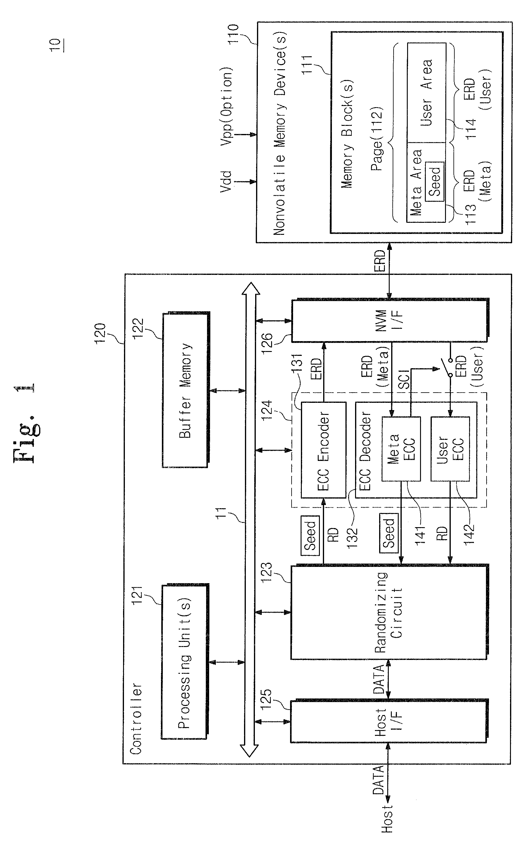
[0049]FIG. 1 is a block diagram of a memory system according to an exemplary embodiment of the inventive concept. Referring to FIG. 1, a memory system 10 includes at least one nonvolatile memory device 110 and a memory controller 120 controlling the nonvolatile memory device 110.

[0050]The nonvolatile memory device according to an exemplary embodiment of the inventive concept may be implemented as a NAND flash memory, a vertical NAND flash memory, a NOR flash memory, a resistive random access memory (RRAM), a phase-change RAM (PRAM), a magnetoresistive RAM (MRAM), a ferroelectric RAM (FRAM), a spin transfer torque RAM (STT-RAM), or the like. Further, the nonvolatile memory device according to an exemplary embodiment of the inventive concept can be implemented to have a three-dimensional array structure (seeFIG. 3). The inventive concept may be applicable to a flash memory device, in which a charge storage layer is formed of a conductive floating gate, and a charge trap flash (CTF) me...


PUM


Abstract

Disclosed is an error correcting method which includes detecting an error of meta data having a seed used to randomize user data; correcting the error of the meta data when the error is detected from the meta data; receiving the user data based upon seed confirmation information associated with an error existence of the seed or an error correction result of the seed; detecting an error of the user data; and correcting the error of the user data when the error is detected from the user data.

Description

CROSS-REFERENCE TO RELATED APPLICATIONS[0001]This application claims the priority, under 35 U.S.C. §119, of Korean Patent Application No. 10-2011-0041679 filed May 2, 2011, the entirety of which is incorporated by reference herein.TECHNICAL FIELD [0002]Exemplary embodiments relate to a memory system and an error correction method.DESCRIPTION OF THE RELATED ART [0003]A flash memory device is a non-volatile memory device, and a type of EEPROM capable of erasing a plurality of memory regions at the same time. A typical EEPROM may enable one memory region to be erased or programmed at the same time. Thus the flash memory device may operate faster and more effectively when systems accessing the flash memory device read and write to different memory regions. All types of EEPROM and the flash memory device may become worn out after the critical number of erase operations due to break down of an electrically insulating film in a memory transistor. The insulating film surrounds a charge stor...

Claims


Application Information

Patent Timeline
IPC IPC(8): H03M13/07G06F11/10
CPCG06F11/1012H03M13/09H03M13/1515H03M13/152H03M13/1525G06F11/0793H03M13/1545H03M13/19H03M13/2903H03M13/2927H03M13/3776H03M13/154G06F11/10H03M13/1105H03M13/611G11C29/42
Inventor KIM, DONGAHN, SEOK-WONKONG, JAEPHILCHOI, MYUNG-SUK
Owner SAMSUNG ELECTRONICS CO LTD
Why Eureka
Try Eureka