Dielectric waveguide filter with direct coupling and alternative cross-coupling

a technology of cross-coupling and dielectric waveguides, applied in waveguides, resonators, electrical equipment, etc., can solve the problems of increasing the length of the filter, not being desirable or possible,

Active Publication Date: 2012-11-15
CTS CORP ELKHART
View PDF1 Cites 51 Cited by
  • Summary
  • Abstract
  • Description
  • Claims
  • Application Information

AI Technical Summary

Benefits of technology

[0008]The present invention relates generally to a waveguide filter comprising a block of dielectric material, a plurality of resonators defined in the block of dielectric material by a plurality of slots defined in the block of dielectric material, the plurality of resonators being arranged on the block of dielectric material in one or more rows and columns; first and second RF signal input / output electrodes defined on the block of dielectric material; and the plurality of resonators and the first and second RF signal input / output electrodes together defining a first direct RF signal transmission path for the transmission of an RF signal through the waveguide filter.

Problems solved by technology

A disadvantage associated with the incorporation of additional resonators, however, is that it also increases the length of the filter which, in some applications, may not be desirable or possible due to, for example, space limitations on a customer's motherboard.

Method used


Image

  • Dielectric waveguide filter with direct coupling and alternative cross-coupling
  • Dielectric waveguide filter with direct coupling and alternative cross-coupling
  • Dielectric waveguide filter with direct coupling and alternative cross-coupling

Examples


first embodiment

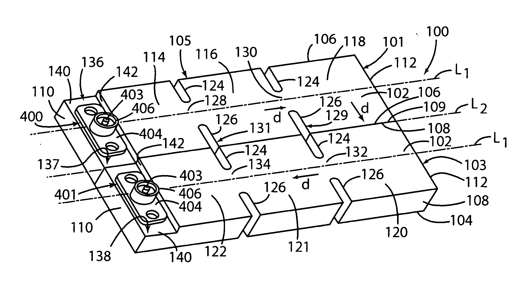
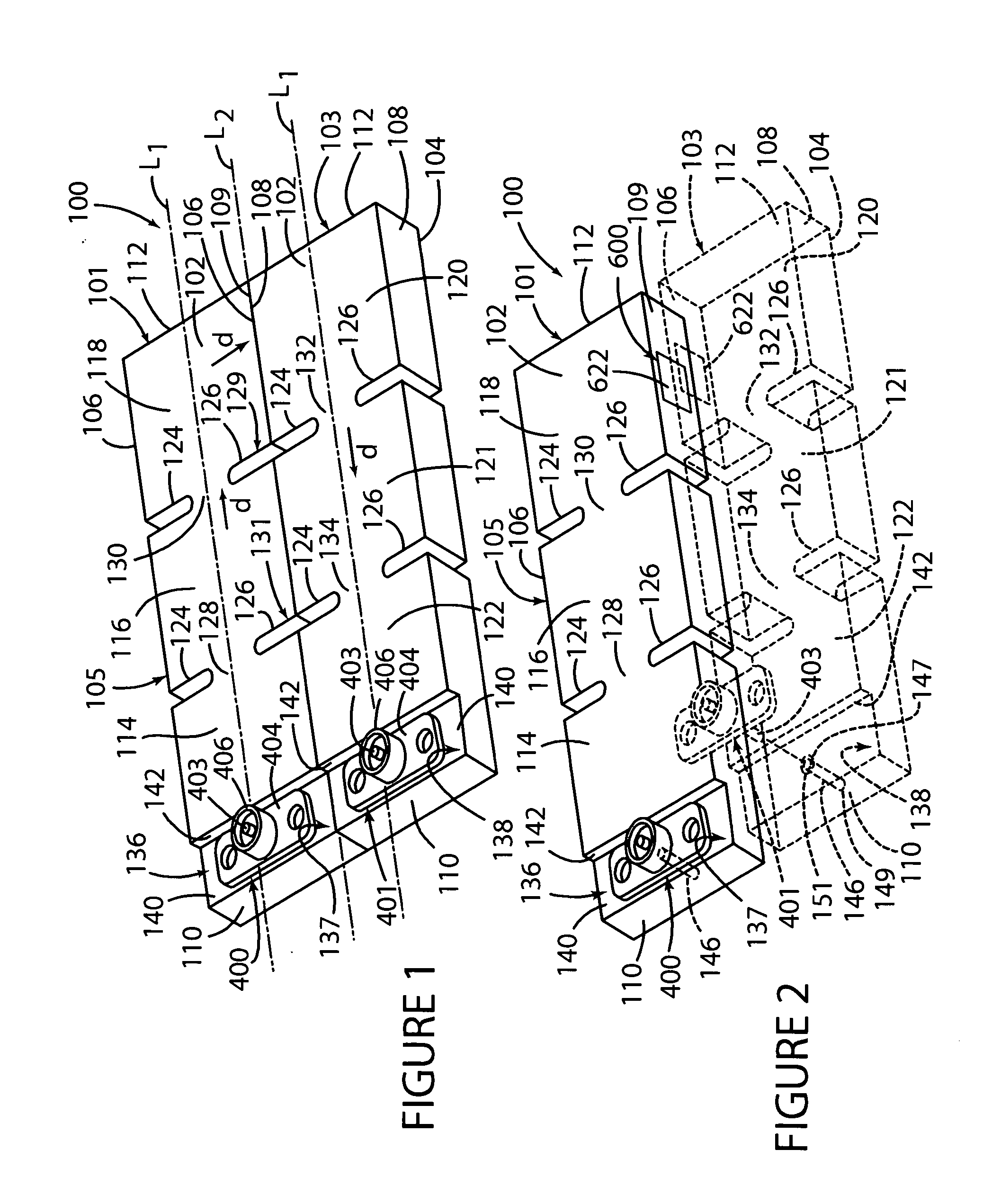
[0045]FIGS. 1 and 2 depict a first embodiment of a ceramic dielectric waveguide filter 100 in accordance with the present invention which incorporates only direct coupling characteristics and in which the attenuation characteristics of the waveguide filter 100 have been increased without increasing the length of the waveguide filter 100 as discussed and described in more detail below.

[0046]Initially, in the embodiment of FIGS. 1 and 2, the waveguide filter 100 is made from a pair of separate generally parallelepiped-shaped monoblocks 101 and 103 which have been coupled and secured together to form the waveguide filter 100 as also described in more detail below.

[0047]Each of the monoblocks 101 and 103 is comprised of a suitable dielectric material, such as for example ceramic; defines a longitudinal axis L1; includes opposed longitudinal horizontal exterior surfaces 102 and 104 extending longitudinally in the same direction as the longitudinal axis L1; opposed longitudinal side verti...

second embodiment

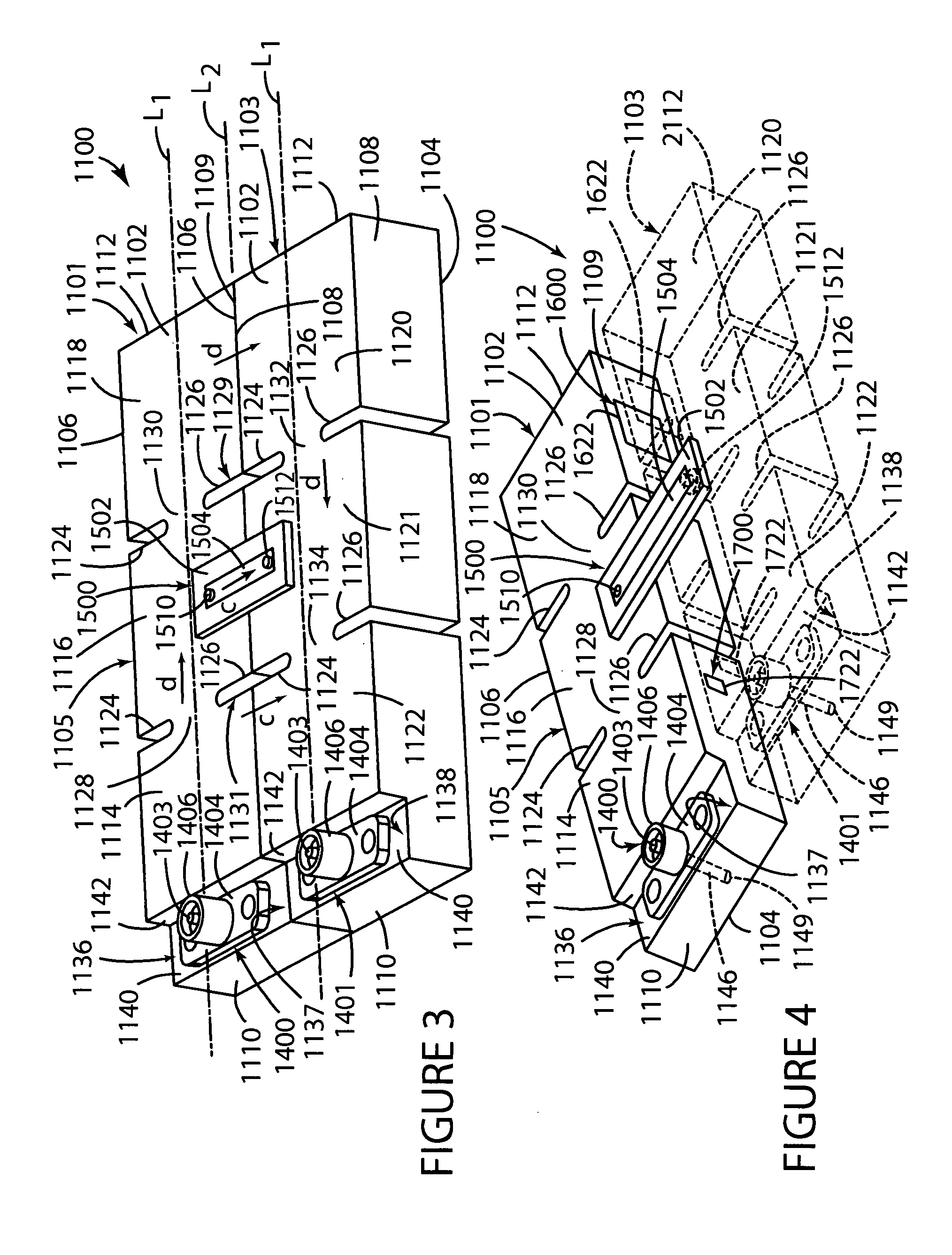
[0086]FIGS. 3 and 4 depict a waveguide filter 1100 which incorporates not only the direct RF signal coupling and transmission features and characteristics of the waveguide filter 100 shown in FIGS. 1 and 2 but also alternate cross-coupling / indirect RF signal coupling and transmission features and characteristics as discussed in more detail below.

[0087]The waveguide filter 1100, in the same manner as the waveguide filter 100 described above and thus incorporated herein by reference is, in the embodiment of FIGS. 3 and 4, made from a pair of separate generally parallelepiped-shaped monoblocks 1101 and 1103 which have been coupled and secured together to form the waveguide filter 1100 as described in more detail below. Each of the monoblocks 1101 and 1103 is comprised of a suitable dielectric material, such as for example ceramic; defines a longitudinal axis L1; includes opposed and spaced-apart longitudinal horizontal exterior surfaces 1102 and 1104 extending longitudinally in the sam...

third embodiment

[0132]FIGS. 5 and 6 depict yet another embodiment of a waveguide filter 2100 in accordance with the present invention which includes all of the elements and features of the waveguide filters 100 and 1100 except that the waveguide filter 2100 includes a step 2137 and, more specifically, steps 2136 and 2138 of varying length and defining shunt zeros as described in more detail below.

[0133]Thus, and as described above with respect to the waveguide filters 100 and 1100 and thus incorporated herein by reference, the waveguide filter 2100 is, in the embodiment shown, made from a pair of separate generally parallelepiped-shaped monoblocks 2101 and 2103 which have been coupled and secured together to form the waveguide filter assembly 2100 as described in more detail below.

[0134]Each of the monoblocks 2101 and 2103 is comprised of a suitable dielectric material, such as for example ceramic; defines a longitudinal axis L1; includes opposed and spaced-apart longitudinal horizontal exterior su...


PUM


Abstract

A dielectric waveguide filter comprising a block of dielectric material including a plurality of resonators defined by a plurality of slots defined in the block of dielectric material. The resonators are arranged on the block of dielectric material in one or more rows and columns. First and second RF signal input/output electrodes are defined on the block of dielectric material. A first direct RF signal transmission path for the transmission of an RF signal is defined by the first and second RF signal input/output electrodes and the plurality of resonators. In one embodiment, internal windows define a first direct RF signal transmission means and additional RF signal transmission means define alternate or cross-coupling paths for the transmission of the RF signal from resonators in one column to resonators in another column. In one embodiment, the filter is comprised of two separate blocks of dielectric material which have been coupled together.

Description

CROSS-REFERENCE TO RELATED AND CO-PENDING APPLICATIONS[0001]This application is a continuation-in-part of, and claims the benefit of the filing date and disclosure of, U.S. application Ser. No. 13 / 103,712 filed on May 9, 2011 and titled “Dielectric Waveguide Filter with Structure and Method for Adjusting Bandwidth”. This application also claims the benefit of the filing date and disclosure of U.S. Provisional Application Ser. No. 61 / 508,987 filed on Jul. 18, 2011. These applications are explicitly incorporated herein by reference as are all references cited therein.FIELD OF THE INVENTION[0002]The invention relates generally to dielectric waveguide filters and, more specifically, to a dielectric waveguide filter with direct coupling and alternative cross-coupling.BACKGROUND OF THE INVENTION[0003]This invention is related to a dielectric waveguide filter of the type disclosed in U.S. Pat. No. 5,926,079 to Heine et al. in which a plurality of resonators are spaced longitudinally along ...

Claims


Application Information

Patent Timeline
Patent Type & Authority Applications(United States)
IPC IPC(8): H01P1/20
CPCH01P1/207H01P1/2002H01P1/208H01P1/2088H01P3/16H01P5/087H01P7/10
Inventor VANGALA, REDDY
Owner CTS CORP ELKHART
Why Eureka
Try Eureka