Eureka AIR delivers breakthrough ideas for toughest innovation challenges, trusted by R&D personnel around the world.

Wafer processing method

Active Publication Date: 2012-11-15
DISCO CORP
View PDF1 Cites 13 Cited by
  • Summary
  • Abstract
  • Description
  • Claims
  • Application Information

AI Technical Summary

Benefits of technology

[0006]However, the grinding strain has a gettering effect such that it attracts heavy metal atoms such as copper atoms to the back side of the wafer to prevent the movement of the heavy metal atoms toward the front side of the wafer (where the devices are formed), thereby suppressing a reduction in function of each device. Accordingly, when the back side of the wafer is polished to remove the grinding strain, the gettering effect of the grinding strain is lost to cause a reduction in function of each device.
[0007]It is therefore an object of the present invention to provide a wafer processing method which can ensure a sufficient die strength of each device constituting a wafer and can also produce a sufficient gettering effect.
[0009]According to the present invention, the silicon nitride film having a thickness of 6 to 100 nm is formed on the polished back side of the wafer from which a grinding strain has been removed. Accordingly, each device constituting the wafer can ensure a sufficient die strength and a sufficient gettering effect. Further, it is confirmed from a test that when the thickness of the silicon nitride film is 200 nm or more, the die strength of each device becomes less than 1000 MPa as an acceptable limit and that when the thickness of the silicon nitride film is less than 6 nm, a sufficient gettering effect cannot be exhibited. Accordingly, by setting the thickness of the silicon nitride film on the back side of each device to 6 to 100 nm, each device can ensure a sufficient die strength greater than an acceptable limit and can also ensure a sufficient gettering effect.

Problems solved by technology

However, the grinding strain has a gettering effect such that it attracts heavy metal atoms such as copper atoms to the back side of the wafer to prevent the movement of the heavy metal atoms toward the front side of the wafer (where the devices are formed), thereby suppressing a reduction in function of each device.
Accordingly, when the back side of the wafer is polished to remove the grinding strain, the gettering effect of the grinding strain is lost to cause a reduction in function of each device.
Further, it is confirmed from a test that when the thickness of the silicon nitride film is 200 nm or more, the die strength of each device becomes less than 1000 MPa as an acceptable limit and that when the thickness of the silicon nitride film is less than 6 nm, a sufficient gettering effect cannot be exhibited.

Method used


Image

  • Wafer processing method
  • Wafer processing method
  • Wafer processing method

Examples


example 1

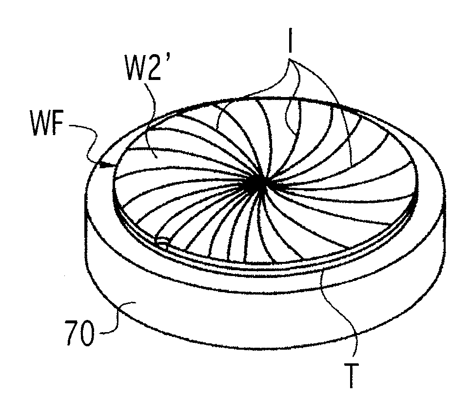
[0031]A test was conducted to obtain the thickness of the silicon nitride film for suitably ensuring the die strength and the gettering effect of each device D. More specifically, the back grinding step, the back polishing step, and the silicon nitride film forming step mentioned above were performed to obtain various samples of the wafer WF in which silicon nitride films having different thicknesses were formed on the back sides of the samples. These samples were used to conduct a gettering effect test and a die strength test, thereby examining the relation between the thickness of the silicon nitride film and the die strength and gettering effect of each device. In conducting the above tests, the conditions of the wafer WF were set as follows:

[0032]Wafer: silicon wafer

[0033]Wafer diameter: 8 inches

[0034]Wafer thickness: 500 μm (after polishing the back side of the wafer)

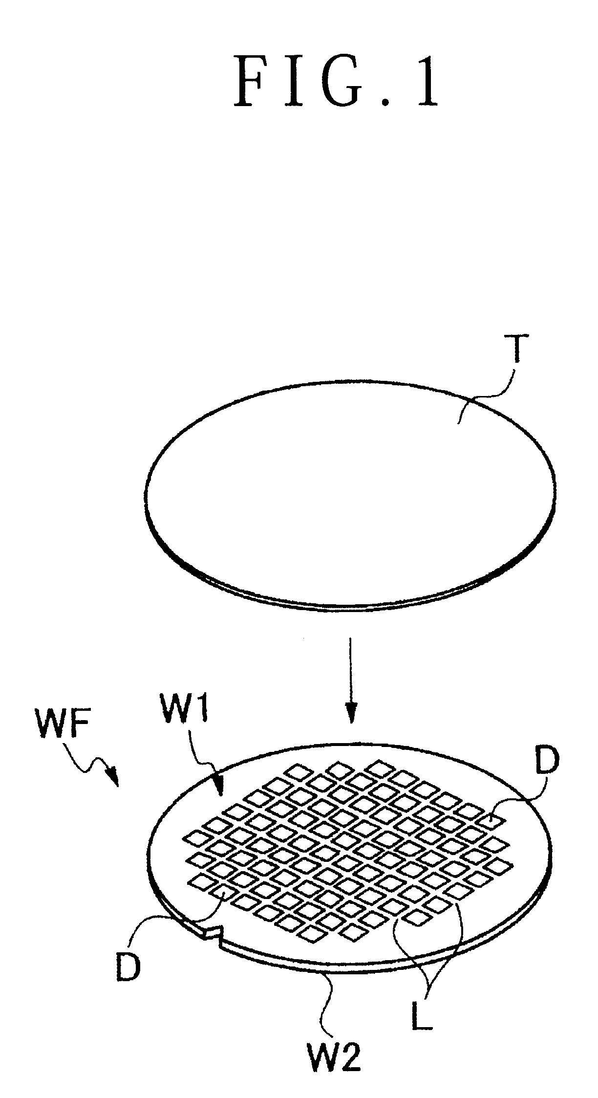
[0035]Chip size: 20 mm×20 mm

[0036]Number of chips per wafer: 61 (see FIG. 10)

(1) Gettering Effect Test

(A) Silico...


PUM

PropertyMeasurementUnit
Nanoscale particle sizeaaaaaaaaaa

Abstract

In a wafer processing method, the back side of a wafer having a plurality of devices on the front side thereof is ground, thereby reducing the thickness of the wafer to a predetermined thickness. The back side of the wafer is polished after performing the back grinding step, thereby removing a grinding strain, and a silicon nitride film is formed on the back side of the wafer. The thickness of the silicon nitride film to be formed in the silicon nitride film forming step is set to 6 to 100 nm. Thus, the silicon nitride film having a thickness of 6 to 100 nm is formed on the polished back side of the wafer from which a grinding strain has been removed. Accordingly, each device constituting the wafer can ensure a sufficient die strength and a sufficient gettering effect.

Description

BACKGROUND OF THE INVENTION[0001]1. Field of the Invention[0002]The present invention relates to a wafer processing method which can provide a sufficient die strength and gettering effect on each device constituting a wafer.[0003]2. Description of the Related Art[0004]A plurality of devices such as ICs and LSIs are formed on the front side of a wafer so as to be partitioned by a plurality of crossing division lines. The back side of the wafer is ground to reduce the thickness of the wafer to a predetermined thickness. Thereafter, the wafer is divided into the individual devices by using a dicing apparatus and the devices thus obtained are used for various electronic equipment or the like. Further, a package device also called an MCP (Multi-Chip Package) generally improved in function is also put to practical use (see Japanese Patent Laid-open No. 2009-26992, for example). This package device is fabricated by grinding the back sides of plural wafers to reduce the thickness of each wa...

Claims


Application Information

Patent Timeline
IPC IPC(8): H01L21/304
CPCH01L21/304H01L21/3221H01L21/0217H01L21/02266C23C14/34H01L21/30625C23C14/0036C23C14/0652H01L21/78
Inventor HARADA, SEIJIKOBAYASHI, YOSHIKAZU
Owner DISCO CORP
Why Eureka
Eureka Blog
Learn More