
Method of manufacturing electrophoretic display device

a technology of electrophoretic display and manufacturing method, which is applied in the direction of manufacturing tools, instruments, optical elements, etc., can solve the problems of degrading display quality and unsatisfactory adhesion, and achieves the effects of low cost, simple process and easy handling

Inactive Publication Date: 2012-11-22
DAI NIPPON PRINTING CO LTD
View PDF7 Cites 8 Cited by
  • Summary
  • Abstract
  • Description
  • Claims
  • Application Information

AI Technical Summary

Benefits of technology

[0008]The present invention has been made in view of the above circumstances. The object of the present invention is to provide a method of manufacturing an electrophoretic display device, which is a simple process but is capable of applying an adhesive agent onto only a partition wall and of reliably adhering the partition wall for forming cells and an electrode substrate to each other.
[0025]By using the adhesive agent made of a thermoplastic material, since the other substrate is reliably adhered by heating the adhesive agent, the adhering portion is prevented from being peeled off even when the other substrate is deformed. Namely, there is generated no gap into which the display medium is undesirably moved. In addition, since there is no possibility that impurities might enter the cell upon adhesion of the other substrate, deterioration of display quality can be avoided. Further, since the heat sealing agent after having been adhered to the other substrate does not have tackiness (stickiness) in a normal temperature, there is also no possibility that the display medium might adhere to the heat sealing agent. Also in this point, deterioration of display quality can be avoided.

Problems solved by technology

Namely, there is a possibility that, after the adhesive agent has been applied to a surface, the surface might have irregularities because of volatilization of solvent of the adhesive agent, which invites unsatisfactory adhesion.
Further, it has been found that, as a result of volatilization of solvent of the adhesive agent, the adhesive agent might enter a cell region or a pixel region that is not desired to be coated therewith, which degrades display quality.

Method used


Image

  • Method of manufacturing electrophoretic display device
  • Method of manufacturing electrophoretic display device
  • Method of manufacturing electrophoretic display device

Examples


Embodiment Construction

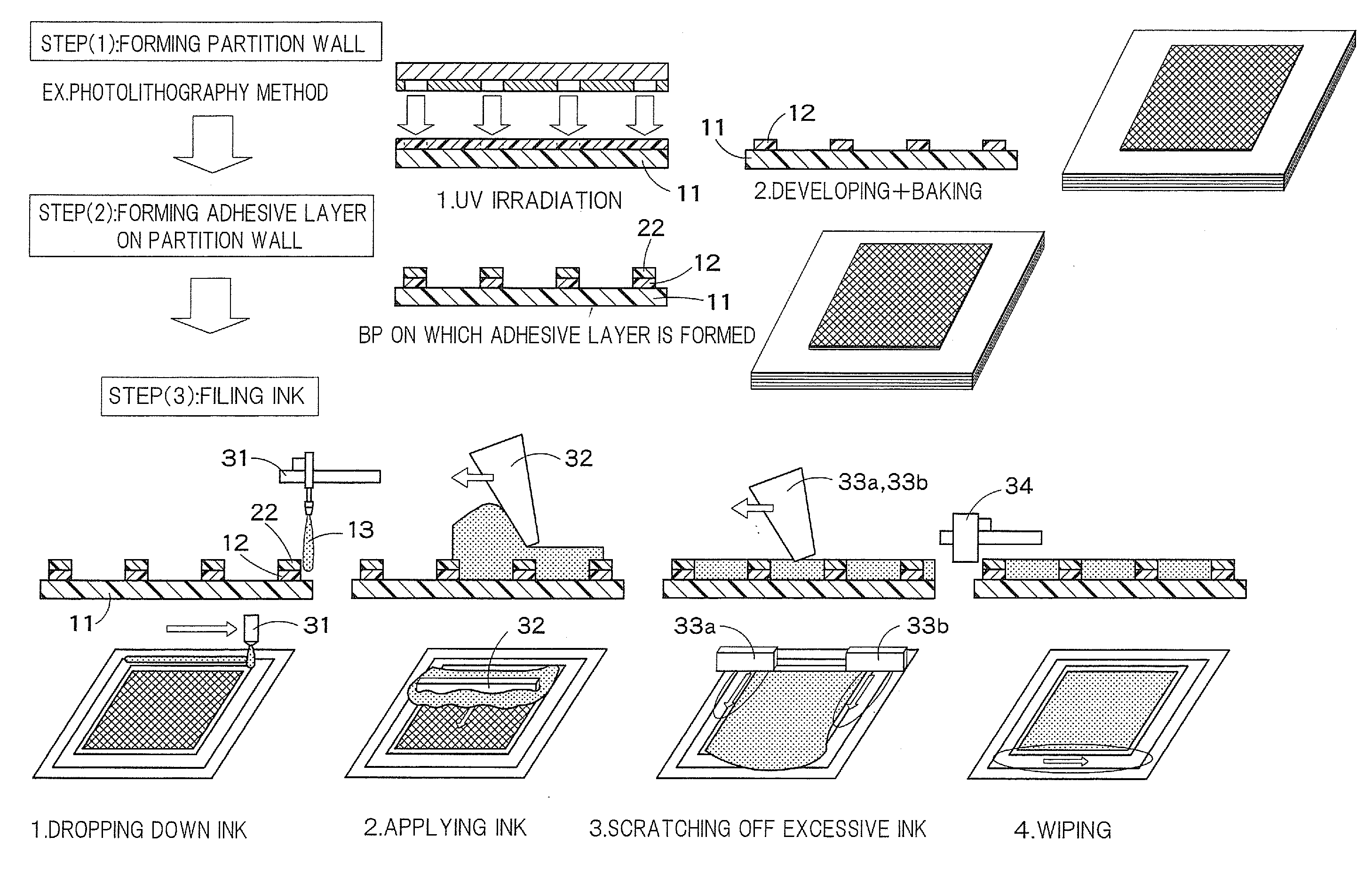
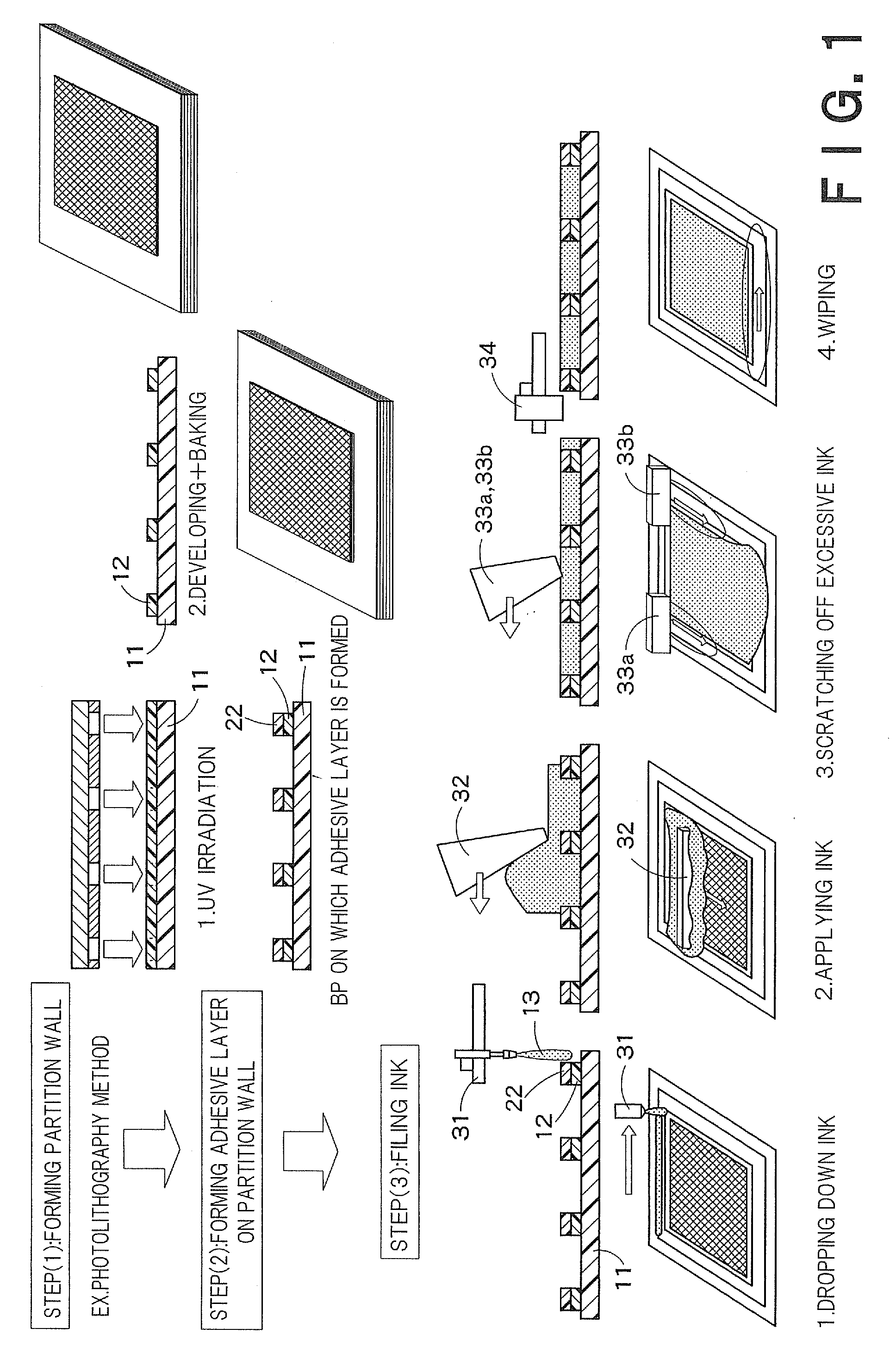
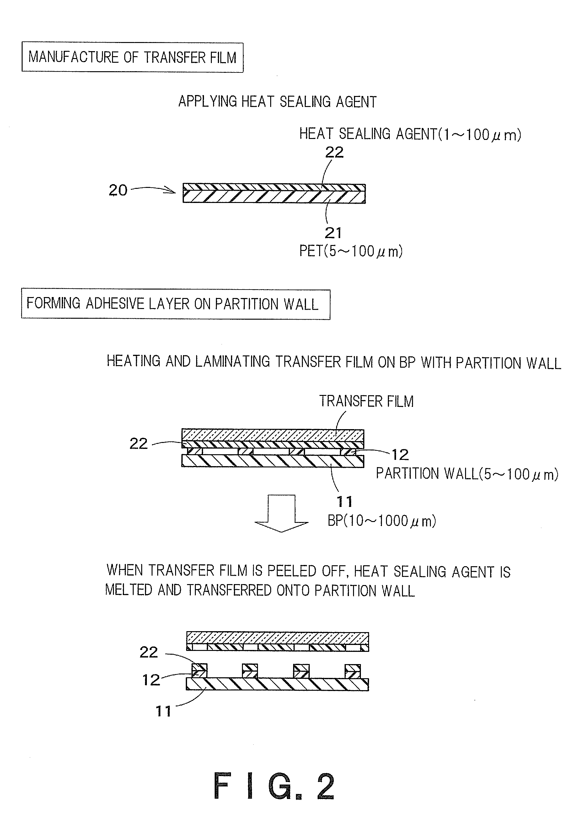
[0031]FIG. 1 is a view schematically showing a first half of a method of manufacturing an electrophoretic display device according to one embodiment of the present invention. As shown in FIG. 1, a partition wall 12 is formed with a predetermined pattern on an upper surface of a lower substrate (one substrate: back plane base member (BP)) that is generally placed horizontally, by means of an ultraviolet (UV) irradiation exposure process, a developing process and a baking process in this order, such as a photolithography method, (partition-wall forming step). The partition wall 12 is a member that defines lower surfaces and side surfaces of a plurality of cells described below.

[0032]A thickness of the partition wall is in a range between 5 μm and 100 μm, and preferably in a range between 10 μm and 50 μm.

[0033]Then, an adhesive layer is formed on the partition wall 12 (adhesive-layer forming step). FIG. 2 is a view schematically showing an example of the adhesive-layer forming step. In...


PUM

PropertyMeasurementUnit
thicknessaaaaaaaaaa
thicknessaaaaaaaaaa
thicknessaaaaaaaaaa

Abstract

A method of manufacturing an electrophoretic device includes: forming a partition wall on a one substrate with a predetermined pattern; forming an adhesive layer on the partition wall; filling each region as a cell, which has been partitioned by the partition wall, with a display medium, after having formed the adhesive layer; and adhering the other substrate onto the adhesive layer on the partition wall so as to enclose the display medium. The forming of the adhesive layer is performed, with the use of a transfer film with a heat sealing agent formed thereon, by heat-transferring the heat sealing agent. The adhering of the other substrate includes heating the heat sealing agent for again softening the heat sealing agent, which has been transferred as the adhesive layer, so as to obtain an adhesive force.

Description

FIELD OF THE INVENTION[0001]The present invention relates to a method of manufacturing an electrophoretic display device applied to electronic paper or the like.BACKGROUND ART[0002]An electrophoretic display device is a device for displaying information, by utilizing electric migration of electrophoretic elements (generally particles that electrically migrate) in an air or a solvent, i.e., movement of particles. In general, an electric migration condition is controlled by applying an electric field between two substrates, so that a desired display can be achieved.[0003]Application of an electrophoretic display device particularly to electronic paper has been widely regarded in recent years. When applied as electronic paper, the electrophoretic display device has advantages such as visibility of printed matter level (easy on the eyes), easiness in rewriting of information, low power of consumption, light weight and so on.[0004]However, in the electrophoretic display device, unsatisfa...

Claims


Application Information

Patent Timeline
Patent Type & Authority Applications(United States)
IPC IPC(8): G02B26/08H05K13/00G02F1/167G02F1/1679
CPCG02F1/167G02F2001/1672Y10T29/49002Y10T29/5313G02F2202/28G02F1/1681G02F1/1679
Inventor IKEGAMI, KANAMIMORIZUMI, DAIGO
Owner DAI NIPPON PRINTING CO LTD
Learn More