

Wiring structure and method of forming the structure
a wire structure and wire technology, applied in the field of wire structure and wire structure formation method, can solve the problems of poor tddb, em degradation, cu+ diffusion, etc., and achieve the effects of reducing current density, reducing current density, and reducing tddb
- Summary
- Abstract
- Description
- Claims
- Application Information
AI Technical Summary
Benefits of technology
Problems solved by technology
Method used
Image

Examples
Embodiment Construction
[0027]The disclosed embodiments and the various features and advantageous details thereof are explained more fully with reference to the accompanying drawings and the following detailed description.
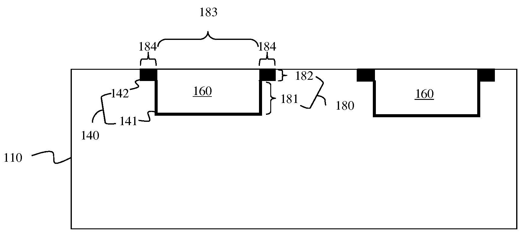
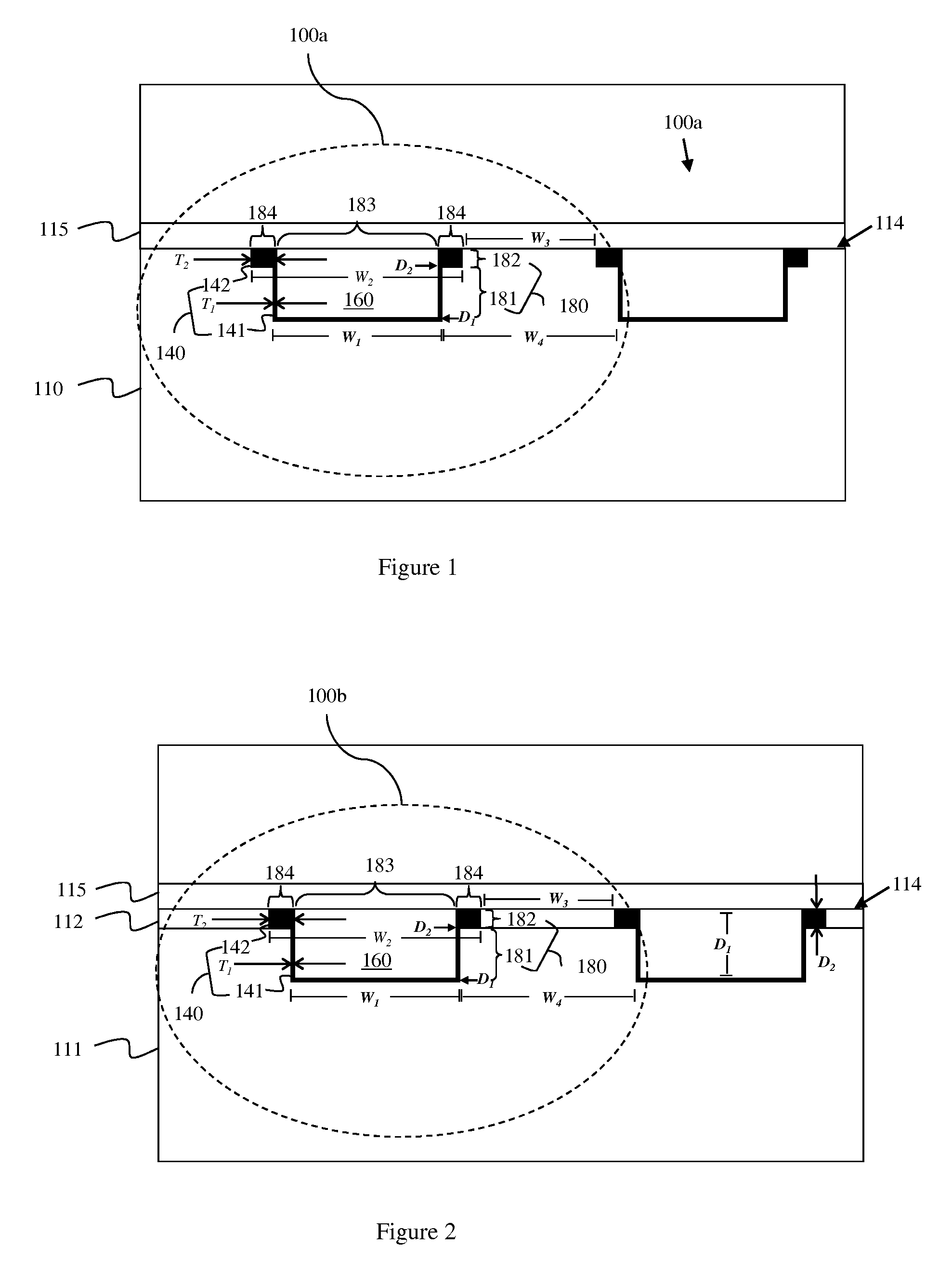
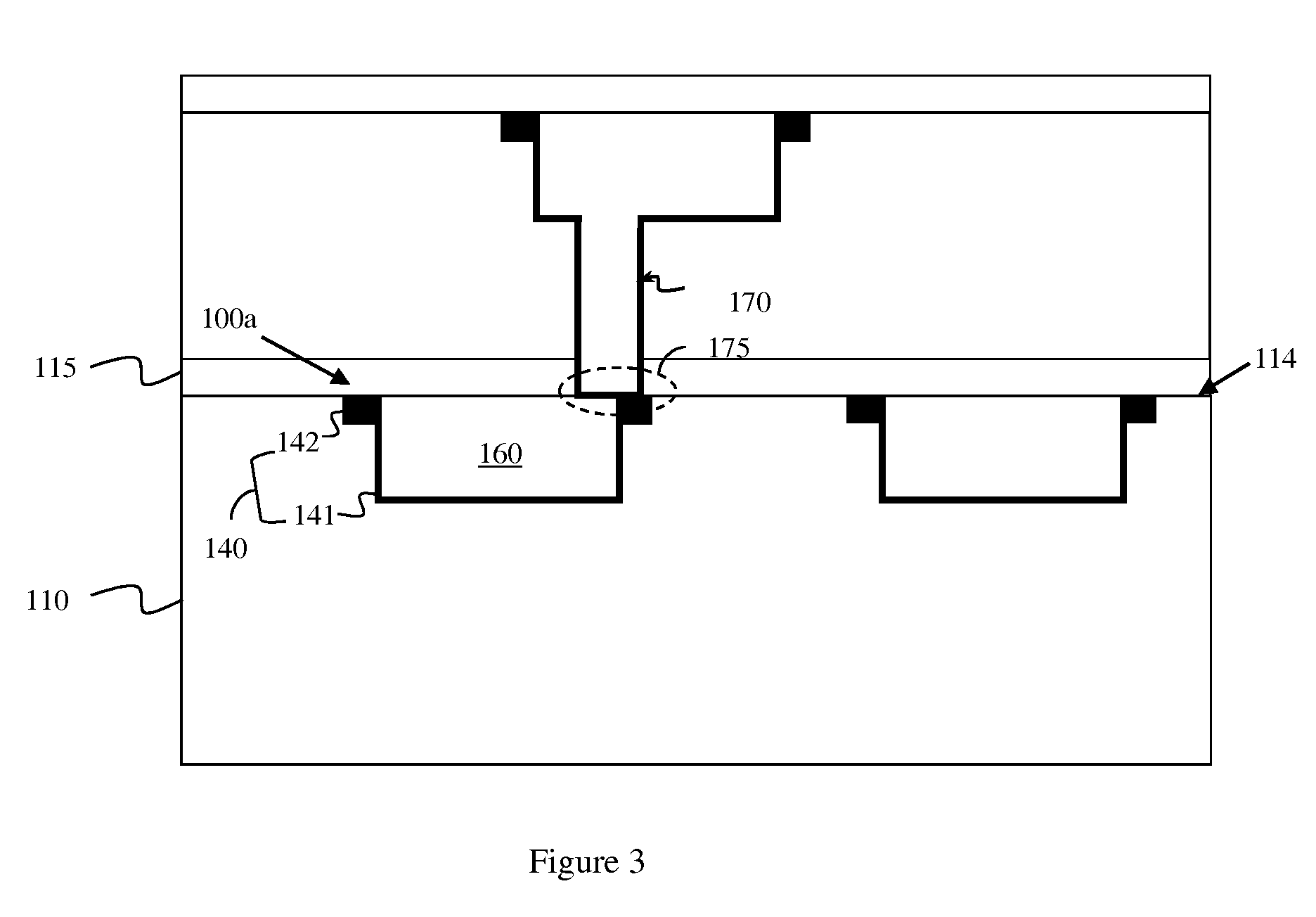
[0028]As mentioned above, back end of the line (BEOL) metal wires have different optimal centering points depending upon the fault mechanism at issue. For example, the optimal ratio of the width of each metal wire to the width of the dielectric material in the space between two adjacent wires (i.e., the optimal wire width to dielectric space width ratio) for opens, for electromigration (EM) and for time dependent dielectric breakdown (TDDB) may be approximately 60:40. Whereas, the optimal wire width to dielectric space width ratio for shorts and for parasitic capacitance may be approximately 40:60. Thus, integrated circuits may be designed with wire width to dielectric space width ratio that balances these competing factors (e.g., a 50:50 wire width to dielectric space width ratio). Howev...
PUM
 Abstract
Description
Claims
Application Information