Light emitting device

a technology of light-emitting devices and lenses, which is applied in the direction of lighting and heating apparatus, lighting support devices, instruments, etc., can solve the problems of increasing unit manufacturing costs, complex manufacturing processes, and increasing manufacturing unit costs, so as to reduce manufacturing time and cost of products, uniform specification, and enhance the degree of freedom in the shape of lenses

Active Publication Date: 2012-11-29
SAMSUNG ELECTRONICS CO LTD
View PDF5 Cites 19 Cited by
  • Summary
  • Abstract
  • Description
  • Claims
  • Application Information

AI Technical Summary

Benefits of technology

[0026]An aspect of the present invention provides a light emitting device capable of reducing a manufacturing time and cost of a product, enhancing a degree of freedom in the shape of a lens in a manufacturing process thereof, implementing a lens shape having a uniform specification, and generating uniform light by reducing a spot phenomenon generated in each of respective light emitting elements.

Problems solved by technology

Thus, in order to implement such a structure, LEDs are manufactured in a package form and then the LED packages are arranged in a row on a substrate such as a PCB so as to be manufactured, and in this case, a manufacturing unit cost is increased due to the manufacturing of the packages.
Here, the manufacturing process is complicated and unit manufacturing cost is increased.
However, a lens formed according to such a method is limited in the configuration.
Namely, the form or shape of the lens is mostly fixed, making it difficult to change the shape of the lens into various forms in consideration of the characteristics of a light emitting device.
Also, individually formed lenses have a certain tolerance in the aspect of standardization, resulting in a severe dispersion in dimensions of respective products, which results in the dispersion of light emitted from the LED chips not being uniform.
In order to prevent such a spot phenomenon, the transmittance of the lens is required to be lowered by a certain numerical value, and in this case, if a lens having a low transmittance is used to prevent the occurrence of a spot phenomenon, the intensity of illumination by the respective LED chips becomes relatively weak, thereby degrading the illumination effect overall.
In order to resolve this problem, a larger number of LED chips are required to be installed densely on the substrate, causing the unit manufacturing cost to be increased.
Meanwhile, a conventional lens is made of a resin such as silicon in order to match a light refractive index, and in this case, silicon is relatively costly, so a method for reducing the usage of silicon is required.

Method used


Image

  • Light emitting device
  • Light emitting device
  • Light emitting device

Examples


Embodiment Construction

[0068]Embodiments of the present invention will now be described in detail with reference to the accompanying drawings.

[0069]The invention may, however, be embodied in many different forms and should not be construed as being limited to the embodiments set forth herein.

[0070]Rather, these embodiments are provided so that this disclosure will be thorough and complete, and will fully convey the scope of the invention to those skilled in the art.

[0071]In the drawings, the shapes and dimensions may be exaggerated for clarity, and the same reference numerals will be used throughout to designate the same or like components.

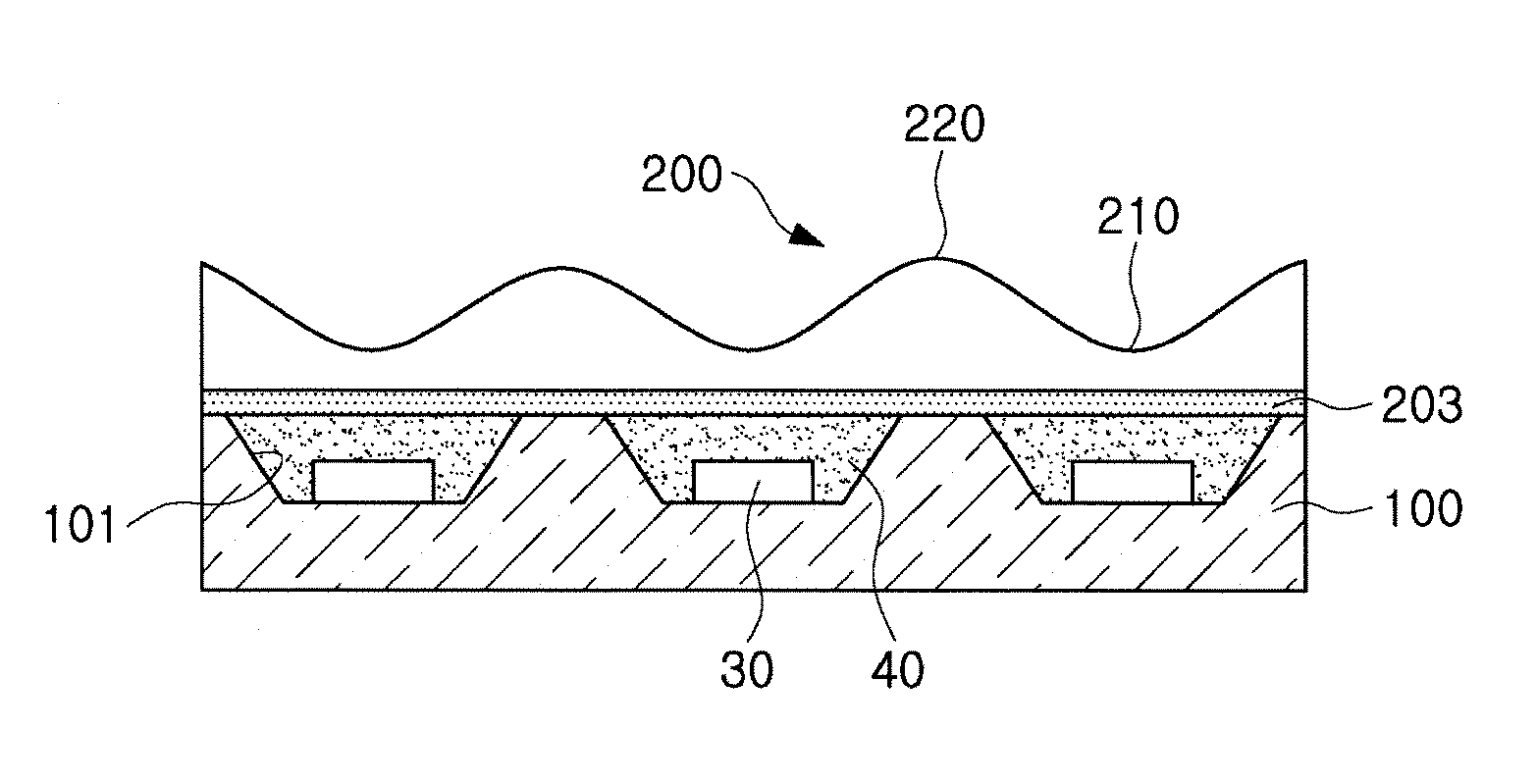
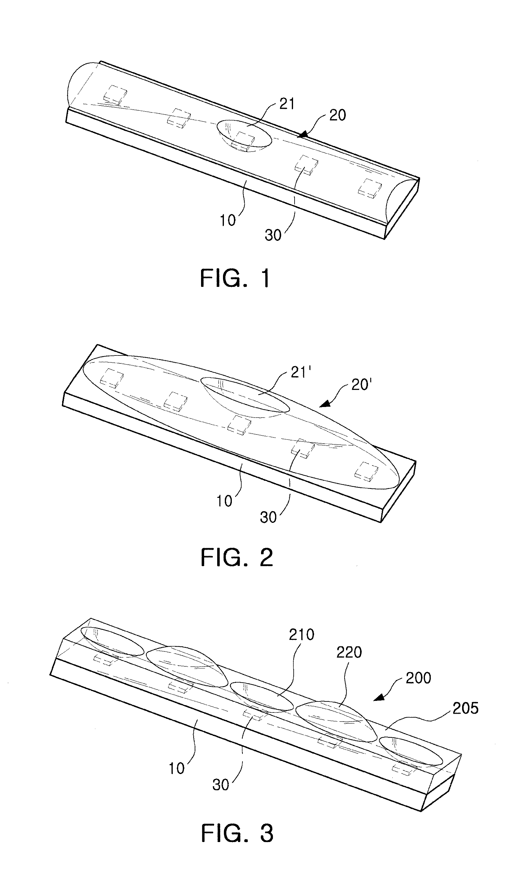
[0072]With reference to FIG. 1, a light emitting device according to an embodiment of the present invention may include a substrate 10, a plurality of light emitting diode (LED) chips 30, light emitting elements, mounted at regular intervals in a lengthwise direction of the substrate 10 on an upper surface of the substrate 10, and a light-transmissive cover 20 installed...


PUM


Abstract

A light emitting device includes: a substrate having a bar shape; a plurality of light emitting elements separately mounted in a lengthwise direction of the substrate on an upper surface of the substrate; and a light-transmissive cover formed to be upwardly convex, having one or more localized concave portions, and installed on the substrate to cover at least two of the plurality of light emitting elements together.

Description

CROSS-REFERENCE TO RELATED APPLICATIONS[0001]This application claims the priority of Korean Patent Application No. 10-2011-0050470 filed on May 27, 2011, in the Korean Intellectual Property Office, the disclosure of which is incorporated herein by reference.BACKGROUND OF THE INVENTION[0002]1. Field of the Invention[0003]The present invention relates to a light emitting device.[0004]2. Description of the Related Art[0005]A light emitting diode (LED), a type of light emitting device which constitutes a light emission source by using a compound material such as GaAs, AlGaAs, GaN, InGaN, AlGaInP, or the like, is a semiconductor device capable of generating light of various colors according to the recombination of electrons and holes at p and n type semiconductor junctions when current is applied thereto.[0006]An LED is environmentally-friendly, has a fast response time in the range of a few nano-seconds to thus be effective for a video signal stream, and is available for impulsive drivi...

Claims


Application Information

Patent Timeline
Patent Type & Authority Applications(United States)
IPC IPC(8): F21V9/16H01L33/50F21V21/00F21V9/00F21V7/00
CPCH01L25/0753H01L33/54H01L33/58H01L2924/0002H01L2924/00G02B19/0066G02B19/0014
Inventor YOU, JAE SUNGSONG, JONG SUP
Owner SAMSUNG ELECTRONICS CO LTD
Why Eureka
Try Eureka