Signal Wiring Board and Signal Transmission Circuit

a signal transmission circuit and signal wiring technology, applied in the field of signal wiring, can solve the problems of increasing the cost of manufacturing the signal wiring board, deteriorating the plugging-unplugging durability of the connector pin, and deteriorating the signal propagation characteristics, so as to reduce the length of the through hole, maintain the plugging-unplugging durability, and reduce the length of the stub.

Inactive Publication Date: 2012-11-29
HITACHI LTD
View PDF5 Cites 35 Cited by
  • Summary
  • Abstract
  • Description
  • Claims
  • Application Information

AI Technical Summary

Benefits of technology

[0015]An object of the present invention, which has been made in order to solve the mentioned problems, is to reduce a length of a stub for a through hole connecting to a signal wiring while maintaining plugging-unplugging durability of a connector pin connecting to a signal wiring board.
[0017]The signal wiring board according to the present invention reduces the length of the through hole connecting to the inner-layer signal wiring, thereby reducing the stub length. The other through holes that do not connect to the inner-layer signal wiring are formed to be longer, so that the connector pins can be inserted deeper in the other through holes, thereby maintaining a plugging-unplugging durability.

Problems solved by technology

Consequently, the through hole has a redundant length which becomes a stub, and thus the signal propagation characteristics are deteriorated.
As a result, a signal wiring connected to such a through hole cannot be used for transmitting a high speed transmission signal, so that an additional signal wiring for a high speed transmission signal or a signal layer for installing this additional signal wiring is required, resulting in increase in cost of manufacturing the signal wiring board.
Such a connector pin having a reduced length, however, deteriorates the plugging-unplugging durability of the connector pin, and thus the connector pin inserted in the through hole should be soldered in order to stably install the connector, resulting in increase in cost.
Therefore, the same problem as in JP Patent Application No. 2007-539262 still exists even though the stub length is reduced to some extent.
The signal wirings connected to the connector pins are, however, provided only on the surface of the board, so that the connector pin and the signal wiring cannot connect to each other through an inner-layer wiring, which significantly limits the wiring design.

Method used


Image

  • Signal Wiring Board and Signal Transmission Circuit
  • Signal Wiring Board and Signal Transmission Circuit
  • Signal Wiring Board and Signal Transmission Circuit

Examples


first embodiment

Conclusion

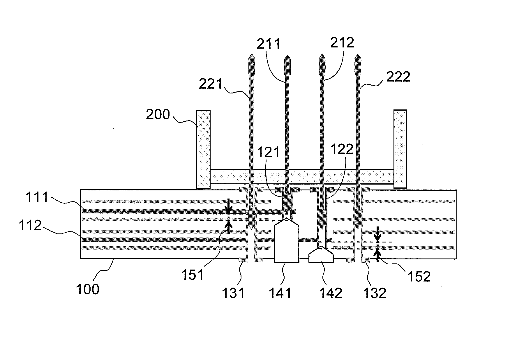
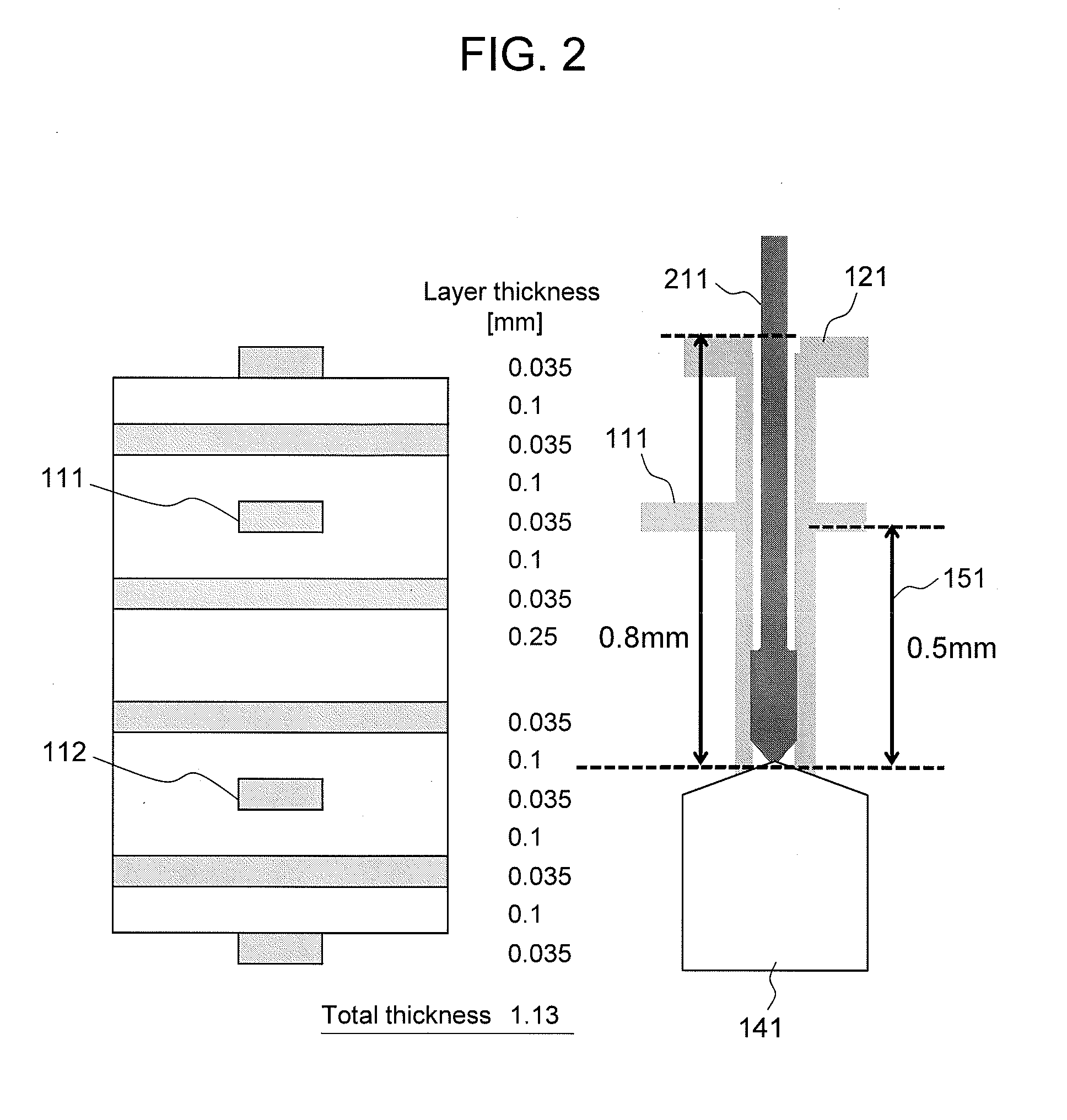
[0051]As described above, in the signal wiring board 100 according to the first embodiment, the through hole for signal pin 121 connecting to the signal wiring 111 is formed to be shorter than the other through holes. The through hole for signal pin 121 has a length in correspondence to the depth of the signal wiring 111, and the signal pin 211 is formed to be shorter than the other connector pins. With this configuration, the signal transmission characteristics over the signal wiring 111 can be maintained to be preferable. Each of the other connector pins has a longer length than that of the signal pin 211, thereby maintaining the plugging-unplugging durability as well as securing movable range in the lateral direction of the connector 200.

[0052]The signal wiring board 100 according to the first embodiment can transmit the high speed transmission signal using the signal wiring 111, which eliminates necessity of providing an additional signal wiring for transmitting the hi...

second embodiment

[0053]FIG. 5 is a sectional side view of the signal wiring board 100 according to the second embodiment of the present invention. In the first embodiment, descriptions have been provided on the example of configuring only the signal pin 211 to be shorter, but such a configuration requires each signal pin of the connector 200 to be processed individually, which is not preferable in the light of the manufacturing cost. In the second embodiment, all the signal pins are formed to have the same length. Specifically, the other connector pins are configured to have the same length as the shorter length of the signal pin 211.

[0054]The through hole for signal pin 122 is connected to the signal wiring 112 at a deeper position in the signal wiring board 100, so that the stub 152 does not become longer even if the signal pin 212 is formed to be shorter. Accordingly, the second embodiment can achieve the same effect as that of the first embodiment, and this configuration is advantageous in the l...

third embodiment

[0055]In the first and second embodiments, descriptions have been provided on the example of reducing the stub lengths by the back drill holes 141, 142 after forming the through holes extending through the signal wiring board 100, but the method of reducing the stub length is not limited to this. Other examples of manufacturing the signal wiring board 100 having a reduced stub length may include the following methods.

(Method 1 of Reducing Stub Length)

[0056]Signal wiring boards having via-holes and inner-layer wirings may be laminated so as to produce a multilayered wiring board. If the boards are laminated such that positions of through holes of each board are aligned with each other, through holes extending through the boards can be formed. If the boards are laminated such that the positions of through holes of each board disagree with each other, the signal wiring board having via-holes extending to intermediate positions in the laminated board can be obtained. Adjustment of the l...


PUM


Abstract

The present invention maintains plugging-unplugging durability of connector pins for connecting to a signal wiring board, as well as reduces a stub length of a through hole connecting to a signal wiring. In the signal wiring board according to the present invention, a through hole connecting to the inner-layer signal wiring is formed to be shorter than the other through holes. A through hole in which a connector pin connecting to the inner-layer signal wiring is inserted is formed to have a length corresponding to a depth of the inner-layer signal wiring.

Description

CLAIM OF PRIORITY[0001]The present application claims priority from Japanese patent application JP 2011-118749 filed on May 27, 2011, the content of which is hereby incorporated by reference into this application.BACKGROUND OF THE INVENTION[0002]1. Field of the Invention[0003]The present invention relates to a signal wiring board implementing signal wirings for electric signal transmission.[0004]2. Background Art[0005]Due to the recent high performance enhancement of electronic equipment, signal transmission speed among electronic components such as LSIs (large scale integrations) implemented in various electronic equipment has been doubling every three years. Particularly in a backplane used in a large scale data processor such as a server and a router, it has been predicted that transmission speed over 25 Gbps (gigabits per second) that is a limit of electric transmission will be required by 2013.[0006]As signal transmission speed increases, transmission loss in a connector for co...

Claims


Application Information

Patent Timeline
Patent Type & Authority Applications(United States)
IPC IPC(8): H05K1/11H01R12/00
CPCH05K1/0251H05K1/115H05K2203/0207H05K2201/10295H05K3/0047
Inventor MURAOKA, SATOSHIYAGYU, MASAYOSHI
Owner HITACHI LTD
Why Eureka
Try Eureka