Nano-sensor array

a technology of nano-sensors and arrays, applied in the field of chemical and biological particle detection, can solve the problems of low signal to noise ratio (snr) of devices, inability to provide real-time monitoring of electrical biosensors, and inability to detect biological particles

Active Publication Date: 2012-11-29
THE BOARD OF TRUSTEES OF THE LELAND STANFORD JUNIOR UNIV
View PDF3 Cites 38 Cited by
  • Summary
  • Abstract
  • Description
  • Claims
  • Application Information

AI Technical Summary

Benefits of technology

[0009]In one embodiment, a method is provided for the manufacture of a nano-sensor array. A base is provided along with a plurality of nano-sensors. Each of the plurality of nano-sensors is formed by forming a first nanoneedle along a surface of the base, forming a dielectric on the first nanoneedle, and forming a second nanoneedle on the dielectric layer. The first nanoneedle of each sensor has a first end adjacent to a region of the base. The second nanoneedle is separated from the first nanoneedle by the dielectric and has a first end adjacent the first end of the first nanoneedle. The plurality of nano-sensors and the fluidic channel are configured and arranged with the first ends in the region to facilitate sensing of targeted matter in the region.

Problems solved by technology

Although sensitive and accurate, these procedures can take as long as several days and thus are not useful for organisms that don't grow easily.
While the fluorescent platforms usually have higher sensitivity and signal to noise ratio (SNR) comparing to electrical biosensors, they may not provide real time monitoring possible with electrical biosensors.
The devices usually suffer from low signal to noise ratio (SNR) due to different sources of noise (e.g. electrical, thermal, Flicker, Johnson, etc) and low detection signal (e.g. the signal generated due to a reaction or binding event of a target molecule to the probe molecule is not large enough).
As a result, electrical biosensors exhibit lower sensitivity, in comparison to the some optical detection techniques, which can be detrimental to early stage detection and diagnosis.

Method used


Image

  • Nano-sensor array
  • Nano-sensor array
  • Nano-sensor array

Examples


Embodiment Construction

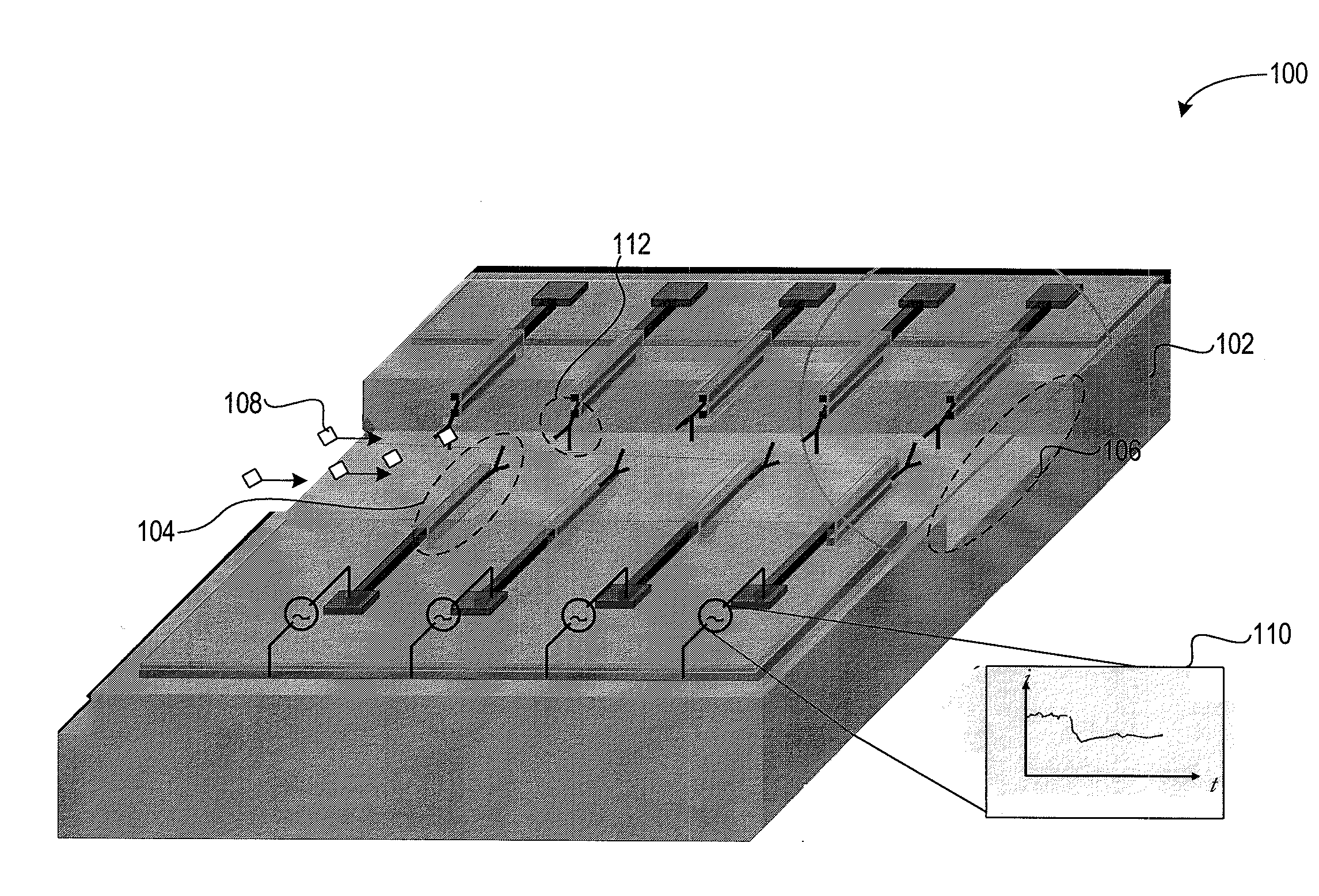
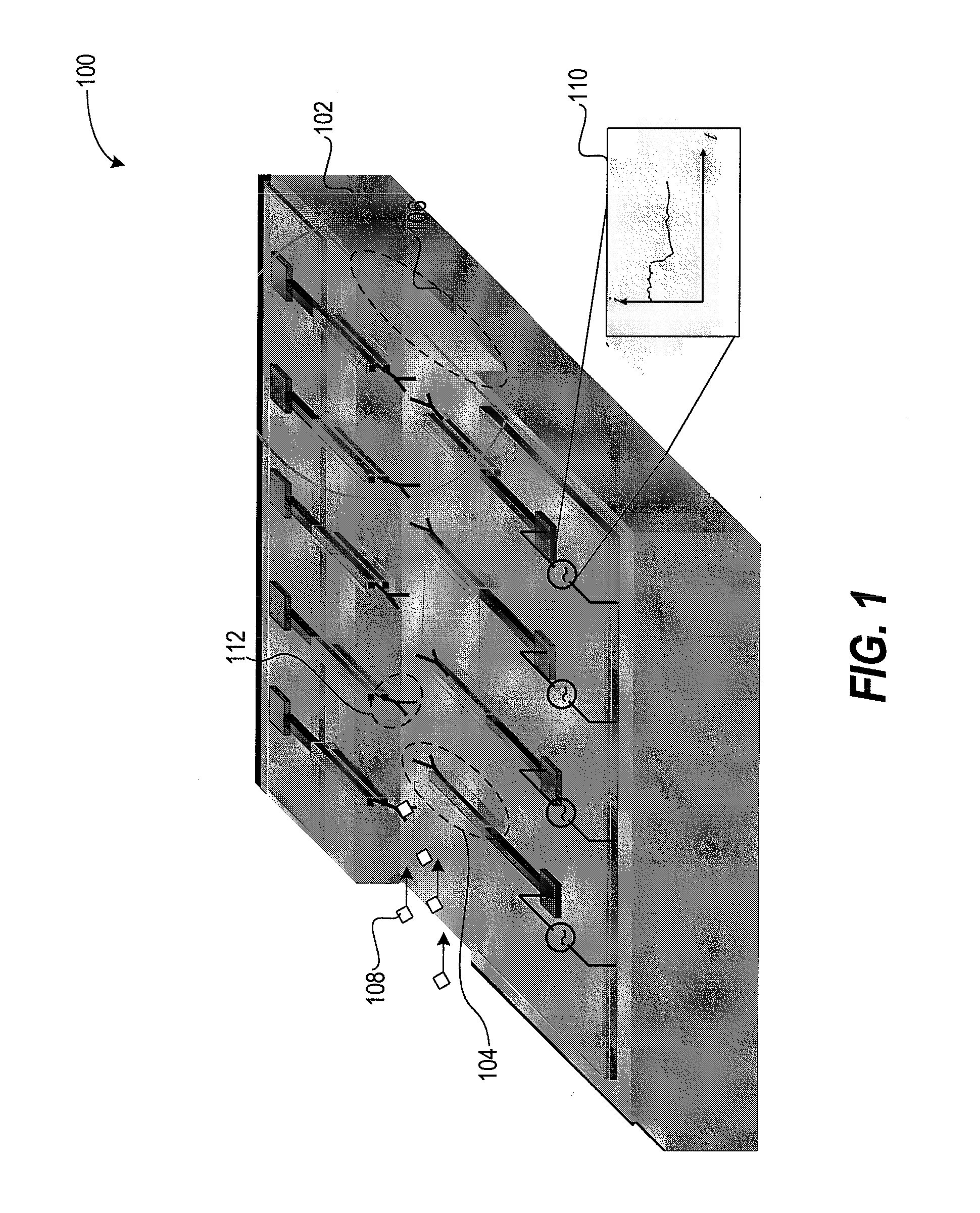
[0031]In one or more embodiments, a cost effective nano-sensor array is provided having a plurality of horizontal nano-sensors having sensing ends formed above a channel region of a base. The sensing ends of the nano-sensors are configured to bind with target particles present in a sample present in the channel. The unique structure of the horizontal nano-sensors exhibits a change in impedance between two terminals of the nano-sensor in response to the binding of target particles. Using this structure, the presence of target particles of interest may be electrically detected with high sensitivity by measuring the impedance of the sensors. In this manner, target particles may be electrically detected with high sensitivity without the use of fluorophores or other labels. The examples and embodiments discussed herein may be described with reference to the detection of either particles or molecules and such terms are used interchangeably herein.

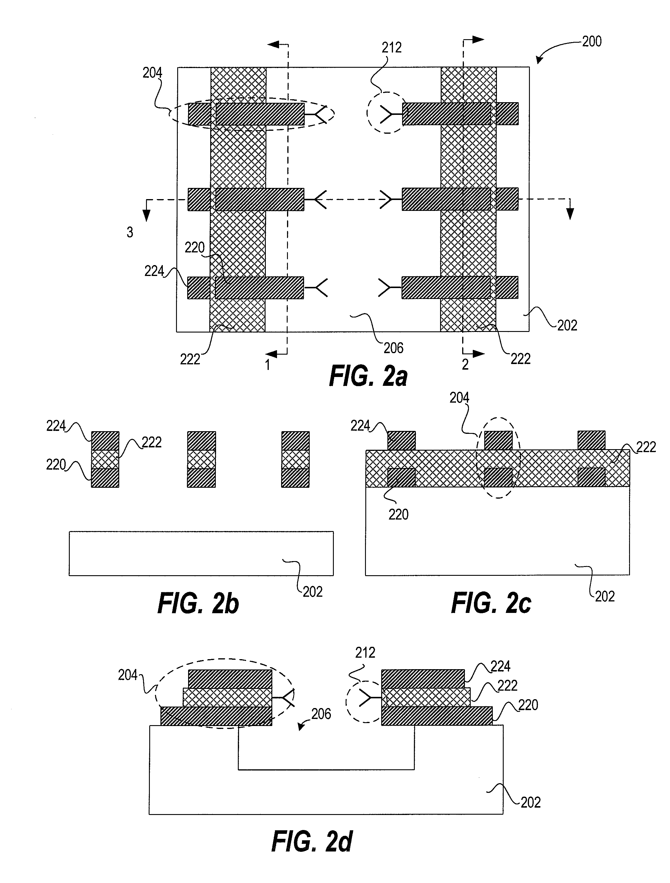
[0032]The horizontal nano-sensors may be f...


PUM

PropertyMeasurementUnit
acceleration voltageaaaaaaaaaa
widthaaaaaaaaaa
widthaaaaaaaaaa

Abstract

In one embodiment, a method is provided for the manufacture of a nano-sensor array. A base having a sensing region is provided along with a plurality of nano-sensors. Each of the plurality of nano-sensors is formed by: forming a first nanoneedle along a surface of the base, forming a dielectric on the first nanoneedle, and forming a second nanoneedle on the dielectric layer. The first nanoneedle of each sensor has a first end adjacent to the sensing region of the base. The second nanoneedle is separated from the first nanoneedle by the dielectric and has a first end adjacent the first end of the first nanoneedle. The base is provided with a fluidic channel. The plurality of nano-sensors and the fluidic channel are configured and arranged with the first ends proximate the fluidic channel to facilitate sensing of targeted matter in the fluidic channel.

Description

STATEMENT OF GOVERNMENTAL SUPPORT[0001]This invention was made with U.S. Government support under National Institutes of Health Grant Number PO1 HG000205. The U.S. Government has certain rights in this invention.FIELD OF THE INVENTION[0002]The present invention relates to chemical and biological particle detection.BACKGROUND OF THE INVENTION[0003]Biosensors are used for detecting the presence of a target chemical or biological agent in a wide variety of applications, such as detection of contaminants in air (e.g., in air quality sensors) or detecting the presence of proteins and nucleic acids in blood samples or other samples. A biosensor measures the presence of various chemical components in a sample contained within a biosensor cell. For example, a biosensor may be used to measure the amount of glucose present in a sample of blood.[0004]Some known methods of detection rely on growth cultures. These methods are based on the ability of pathogenic species to multiply in nutrient-ric...

Claims


Application Information

Patent Timeline
Patent Type & Authority Applications(United States)
IPC IPC(8): C40B30/04B23P11/00C40B60/12
CPCC12Q1/6825Y10T29/49826G01N27/3278G01N33/49B82Y40/00C40B60/12B82Y15/00
Inventor ESFANDYARPOUR, HESAAM
Owner THE BOARD OF TRUSTEES OF THE LELAND STANFORD JUNIOR UNIV
Why Eureka
Try Eureka