High speed lasing device

a high-speed, lasing technology, applied in the direction of laser details, semiconductor lasers, electrical apparatus, etc., can solve the problem of limiting the increase of effective parasitic capacitance related to an oxide layer, and achieve the effect of reducing effective parasitic capacitance, simple and cost-effective manner, and faster and more reliable fiber optical communication systems

Active Publication Date: 2012-12-06
MELLANOX TECHNOLOGIES LTD
View PDF6 Cites 2 Cited by
  • Summary
  • Abstract
  • Description
  • Claims
  • Application Information

AI Technical Summary

Benefits of technology

[0019]Therefore, the problem underlying the present invention is to provide a lasing device for use in directly modulated high-speed fiber optical communication systems, which can be driven at a high-modulation speed, which has a reduced effective parasitic capacitance, and which can be fabricated in a particularly simple and cost-effective manner and at the same time allows for a faster and more reliable fiber optical communication system.

Problems solved by technology

In addition, the guard laser causes a reduction of the carrier injection in the outer region of the diode structure, thereby limiting the increase of the effective parasitic capacitance related to an oxide layer.

Method used


Image

  • High speed lasing device
  • High speed lasing device
  • High speed lasing device

Examples


Embodiment Construction

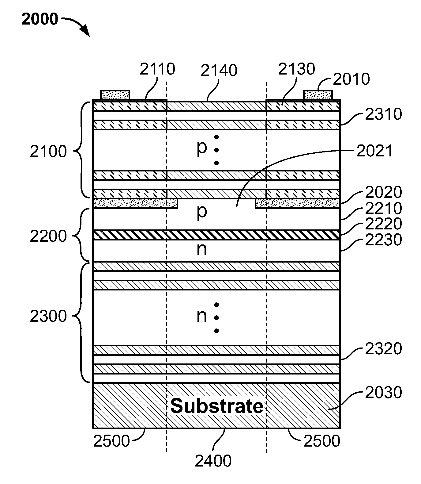
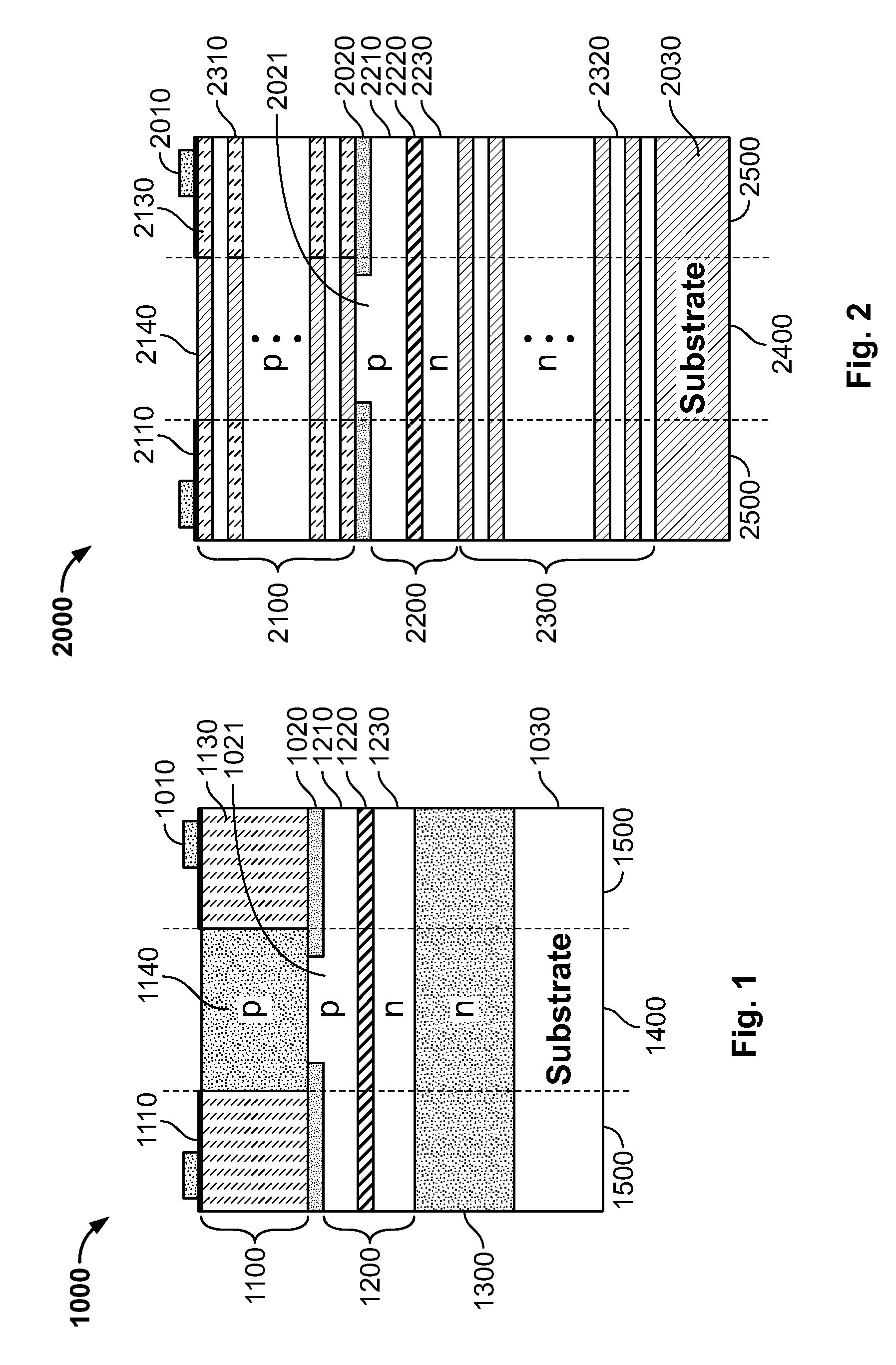
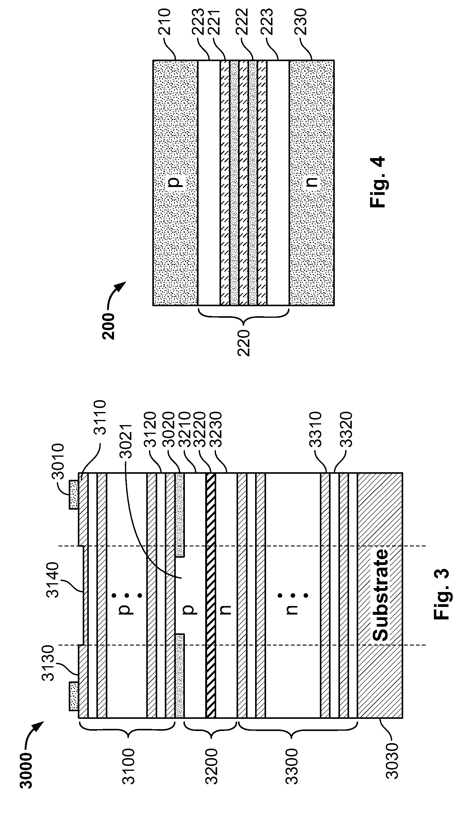
[0046]In the following description, for explanatory purposes, specific details are set forth in order to provide a thorough understanding thereof. However, it may be evident that the present invention can be practiced without these specific details. Furthermore, well known structures and devices are only described in a more general form in order to facilitate the description thereof.

[0047]In the following description the expressions “mirror” and “reflector” are used to indicate the stacks of semiconductor or dielectric layers defining the resonant cavity of the laser. Similarly the expressions “first mirror region” and “first reflector region” are used in the following with the same meaning; and the expressions “second mirror region” and “second reflector region” are used in the following with the same meaning. The expression “gain region” and “cavity spacer” indicate the semiconductor layers sandwiched between the reflectors of the lasing device.

[0048]The problem underlying the pre...


PUM


Abstract

The present invention relates to a lasing device for use in an optical module. The lasing device comprises a first reflector and a second reflector; a confinement layer adapted to confine current within a current-confining aperture; and an active layer between the first and second reflectors. The active layer comprises a main active region aligned with the current confining aperture and an auxiliary active region surrounding the main active region. The second reflector includes a first reflector region arranged on the current-confining aperture and a second reflector region surrounding the first reflector region. The second reflector region and the first reflector are configured to induce stimulated recombination in the auxiliary active region.

Description

BACKGROUND OF THE INVENTION[0001]1. Field of the Invention[0002]The present invention relates to lasing devices for use in high-speed fiber optical communication systems, and more specifically to Vertical Cavity Surface Emitting Lasers (VCSELs) with high modulation bandwidth. Moreover the present invention relates to optical interconnects including lasing devices with high modulation bandwidth. Finally, the present invention relates to a method for manufacturing high-speed lasing devices.[0003]2. Related Art to the Invention[0004]Lasing devices and in particular Vertical Cavity Surface Emitting Lasers commonly used in high-speed communication systems include a cavity sandwiched between two highly reflective mirrors or reflectors so as to form a resonator. The mirrors include several alternating layers of semiconductors of high and low refractive index and are doped with p-type and n-type dopants or impurities, respectively so as to form a p-n or a p-i-n diode junction. In a semicond...

Claims


Application Information

Patent Timeline
Patent Type & Authority Applications(United States)
IPC IPC(8): H01S5/32H01S5/02315
CPCH01S5/0425H01S5/06226H01S5/18311H01S2301/18H01S5/18358H01S5/18375H01S5/18394H01S5/18327H01S5/023H01S5/0233H01S5/0235H01S5/02345H01S5/02315
Inventor CHITICA, NICOLAE PANTAZI
Owner MELLANOX TECHNOLOGIES LTD
Why Eureka
Try Eureka