Switching regulator

a technology of switching regulator and regulator, which is applied in the direction of electric variable regulation, process and machine control, instruments, etc., can solve the problems of an increase in ripple voltage of output voltage vout, oscillation frequency change irrespective, etc., and achieve the effect of reducing the driving loss of switching element 21, boosting efficiency under light load, and suppressing ripple voltag

Inactive Publication Date: 2012-12-13
ABLIC INC
View PDF9 Cites 10 Cited by
  • Summary
  • Abstract
  • Description
  • Claims
  • Application Information

AI Technical Summary

Benefits of technology

[0020]According to the switching regulators of the present invention, a switching operation is performed at an optimum frequency in accordance with the load current Tout, and therefore the driving loss of the switching element 21 reduces. Therefore boosting efficiency under light load can be improved. Further even when the output voltage Vout is set low, the switching frequency is not fixed at a low state. Accordingly, ripple voltage can be suppressed.

Problems solved by technology

The aforementioned conventional switching regulator, however, has the drawback that the oscillation frequency changes irrespective of the load current Tout when the output voltage Vout is set low.
That is, energy feeding cycle becomes long, during which discharging of the output voltage Vout proceeds, thus causing a problem of an increase in ripple voltage of the output voltage Vout.

Method used


Image

  • Switching regulator
  • Switching regulator
  • Switching regulator

Examples


embodiment 1

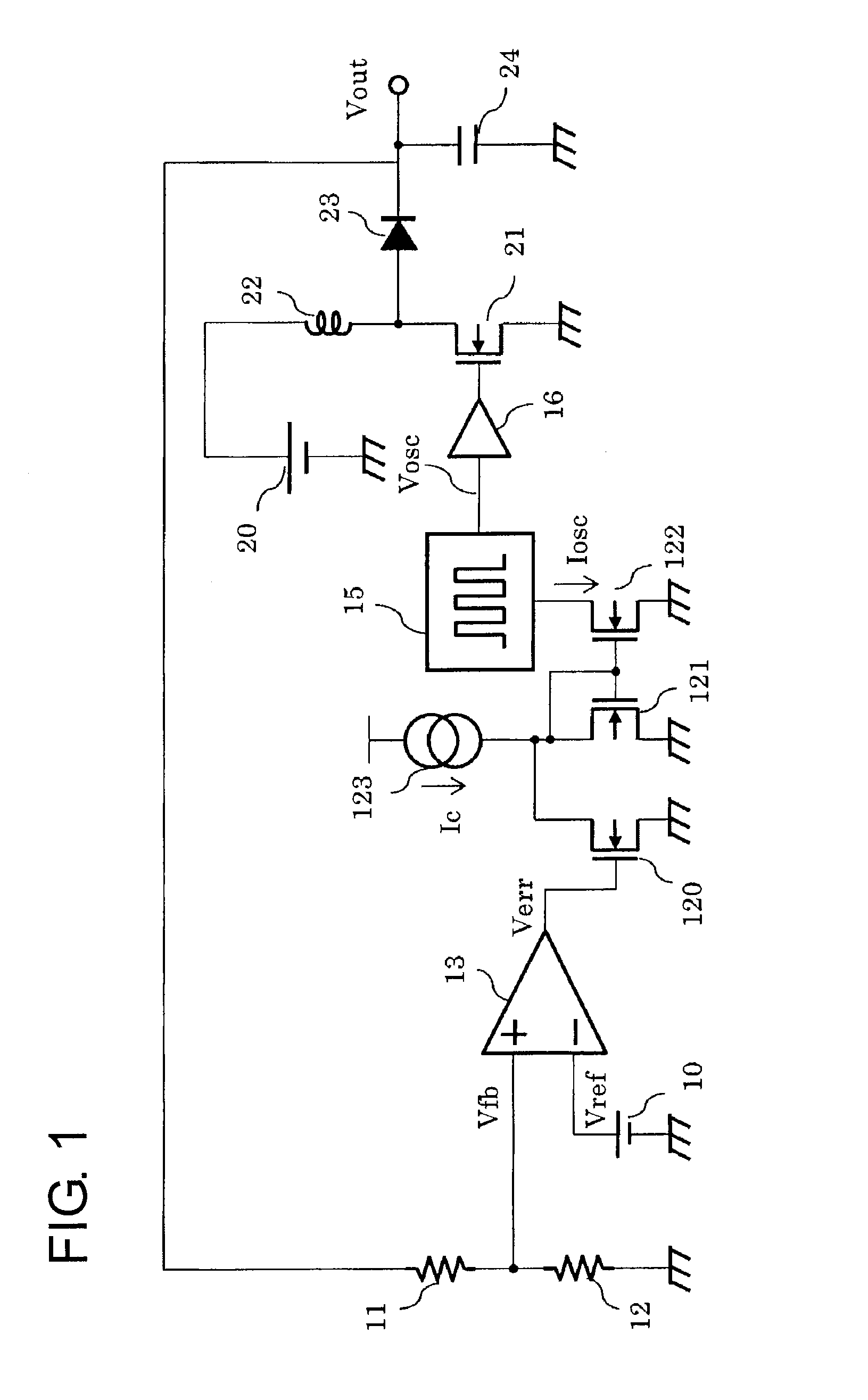
[0026]FIG. 1 is a circuit diagram of a switching regulator that is

[0027]The switching regulator of Embodiment 1 includes: output voltage division resistances 11 and 12; a reference voltage circuit 10; an error amplifier 13; an oscillation circuit 15; a buffer circuit 16; a switching element 21; a coil 22; a diode 23; an output capacity 24; a constant current source 123 and transistors 120, 121 and 122. The constant current source 123 feeds constant current Ic. The oscillation frequency of the oscillation circuit 15 is controlled based on fed bias current Iosc.

[0028]The output voltage division resistances 11 and 12 divide the output voltage Vout and output divided voltage Vfb. The error amplifier 13 compares the divided voltage Vfb with the reference voltage Vref that is output from the reference voltage circuit 10 and amplifies a different voltage thereof to output the same as voltage Verr. Since the divided voltage Vfb is input to a non-inverting input of the error amplifier 13 and...

embodiment 2

[0036]FIG. 2 is a circuit diagram of a switching regulator that is

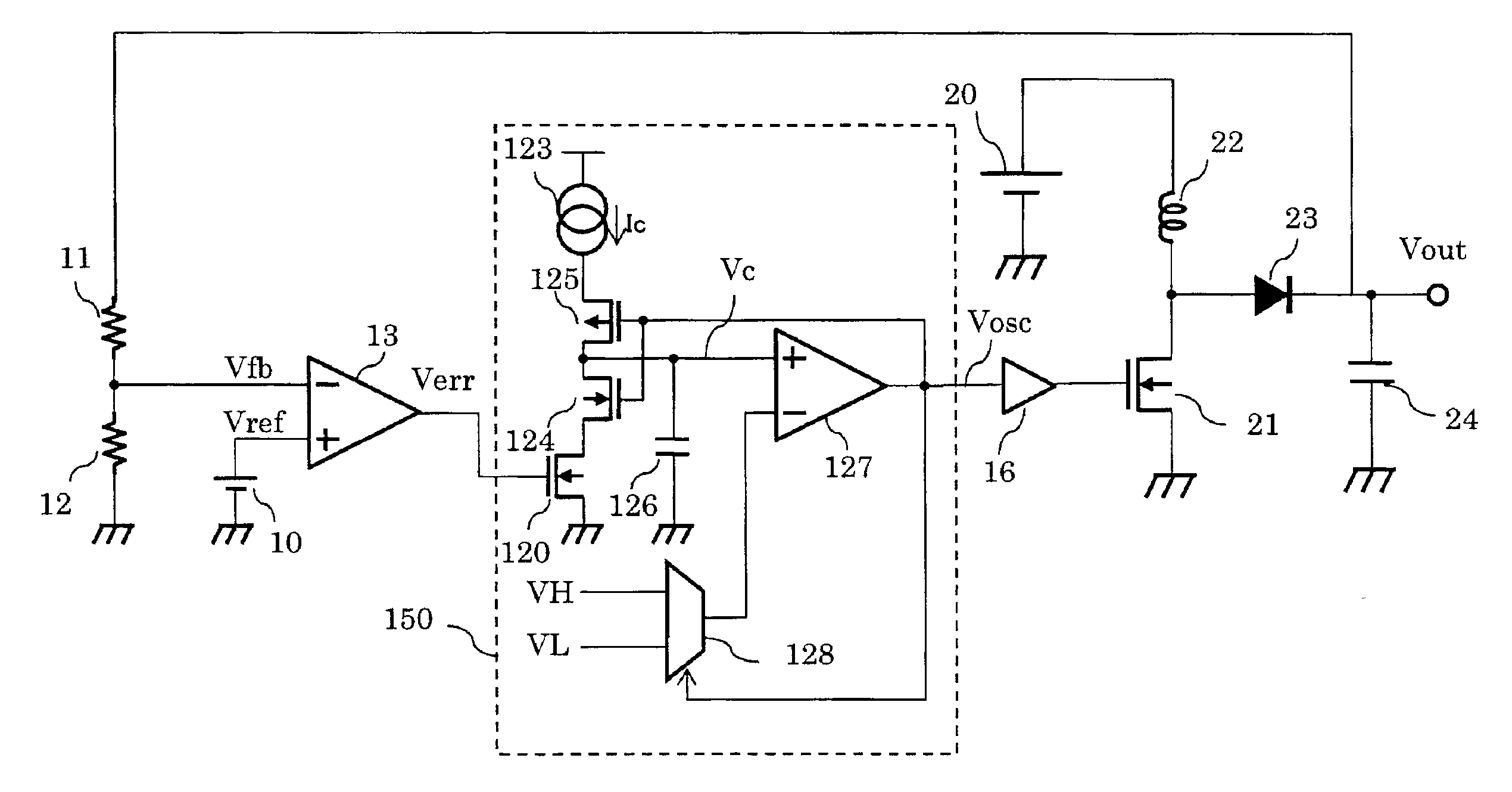
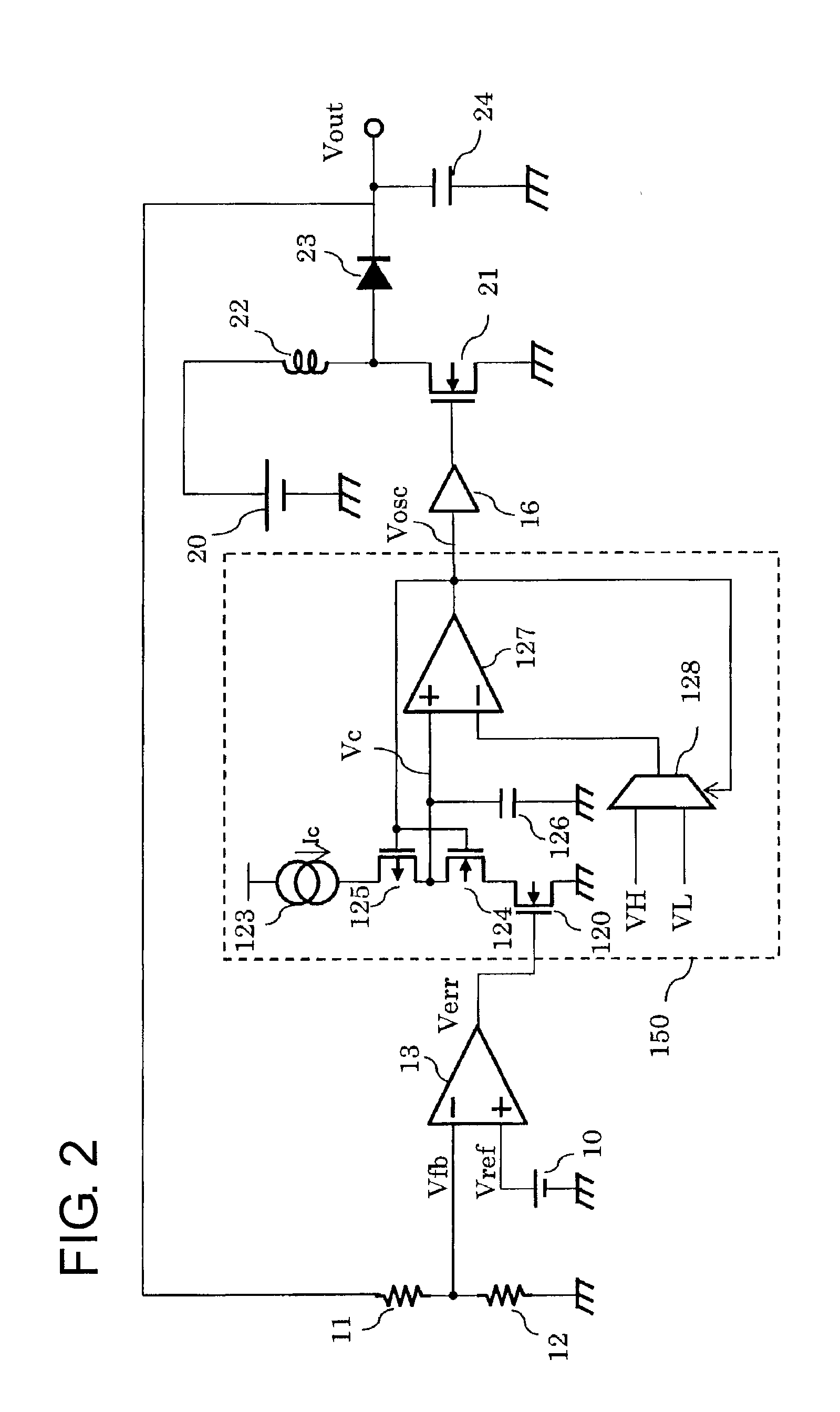
[0037]The switching regulator of Embodiment 2 includes: output voltage division resistances 11 and 12; a reference voltage circuit 10; an oscillation circuit 150; a buffer circuit 16; a switching element 21; a coil 22; a diode 23 and an output capacity 24. The oscillation circuit 150 includes a comparator 127; a capacity 126; a constant current source 123; charge / discharge control elements 120, 124 and 125 and a multiplexer 128.

[0038]The error amplifier 13 has an inverting input terminal to which divided voltage Vfb is input, a non-inverting input terminal to which reference voltage Vref is input and an output terminal connected to the charge / discharge control element 120. The constant current source 123 and the charge / discharge control elements 125, 124 and 120 are connected in series between a power supply and ground. The multiplexer 128 receives reference voltage VL and reference voltage VH as input. The reference ...


PUM


Abstract

In order to provide a switching regulator having high efficiency even under light load, the switching regulator is configured so that ON/OFF of a switching element is controlled by an output signal of an oscillation circuit having an oscillation frequency controlled by an output signal from an error amplifier. Thereby, the oscillation frequency can be suppressed under light load, thus reducing a switching loss.

Description

RELATED APPLICATIONS[0001]This application claims priority under 35 U.S.C. §119 to Japanese Patent Application No. 2011-129399 filed on Jun. 9, 2011, the entire content of which is hereby incorporated by reference.BACKGROUND OF THE INVENTION[0002]1. Field of the Invention[0003]The present invention relates to switching regulators capable of increasing the efficiency under light load.[0004]2. Description of the Related Art[0005]Switching regulators are used as a voltage supply source for various electronic device circuits. One of functions of switching regulators is to output a constant voltage through an output terminal with high conversion efficiency irrespective of voltage fluctuation at an input terminal. It is also important for switching regulators to maintain high conversion efficiency even when an electronic device as a load enters a low power consumption mode such as a stand-by state so that current supplied from the output terminal to the load decreases.[0006]FIG. 4 is a ci...

Claims


Application Information

Patent Timeline
Patent Type & Authority Applications(United States)
IPC IPC(8): G05F1/10
CPCH02M3/156Y02B70/16H02M2001/0035H02M1/0035Y02B70/10H02M1/14H02M3/155
Inventor DEGUCHI, MICHIYASUYOSHIDA, KENJI
Owner ABLIC INC
Why Eureka
Try Eureka